Full company details
Bruker Nano Surfaces
Div. of Bruker Corp.
 5255 E Williams Circle, Suite 2080
Tucson, AZ 85711
United States
Phone: +1 520-741-1044
Fax: +1 520-294-1799
Toll-free: +1 800-873-9750
White Light Interferometry Returns Vital Measurement Values in a Single Shot
Photonics Spectra
May 2025An interferometric approach delivers detailed information on both the film and the substrate surface for improved control over thin-film coatings.ERICA ERICKSON AND ROGER POSUSTA BRUKER NANO SURFACES AND METROLOGY
Obtaining accurate control over film thickness and uniformity is critical
for applications ranging from optics, flexible
electronics, and microelectromechanical systems (MEMS)
manufacturing to semiconductor advanced packaging and energy technologies. Many methods — both contact and noncontact — are used to obtain film thickness measurements. These include stylus profilometry, ellipsometry, and x-ray reflectivity. Each offers benefits that depend largely on the application and application environment.

Courtesy of iStock.com/Wirestock.
In terms of cost-effectiveness and speed of operation, white light interferometry (WLI) offers considerable advantages to system designers and developers. In addition to film thickness and coating uniformity, this characterization technique is effective for defect detection and can provide information on roughness for both film and substrate over large areas.
Critically, WLI can provide these insights in a single measurement that takes only a few seconds. This makes the approach ideal for applications where speed is critical, parts are large, samples are fragile, and where physical contact of the surface can cause damage or there is nonuniform surface texture.
The prospect of gauging numerous parameters via a single-shot technique is especially important. Inspecting only the top of a film coating, for example, does not tell the whole story. As a result, this singular measurement may not be an appropriate determinant of the viability of a given thin film for a given application. And whether the initial substrate is rough or has imperfections can also influence the coating surface (Figure 1). Fundamentally, determining the root cause of film surface texture requires analyses of both substrate surface and film top surface.
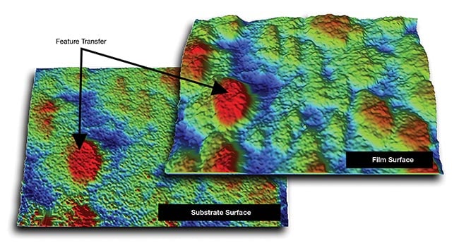
Figure 1. The 3D optical profiling images show feature transfer between the substrate surface and film surface. Courtesy of Bruker Nano Surfaces and Metrology.
WLI enables users to access both the substrate and film surfaces for nonopaque films. This quality, paired with large-area measurement capabilities of up to 15 mm in a single image, makes it invaluable for developers and users of thin films.
Technique basics and advantages
In WLI profilers, interference patterns are generated using split and recombined light waves. These interference patterns are used to calculate surface topography with sub-angstrom-scale resolution. Among other inherent advantages, this technique offers high throughput, a lack of mechanical damage, low maintenance, and deep trench/sidewall capabilities.
WLI uses areal scanning, where everything within the field of view is measured simultaneously. This enables the technique to achieve a higher throughput than the point-by-point profiling method used by stylus profilers. As an optical-only, noncontact, and nondestructive method, WLI also avoids any risk for mechanical damage and does not have consumables. These systems may also self-calibrate, which decreases maintenance requirements.
Another major benefit to the use of WLI is its magnification-insensitive height resolution. WLI profilers use interferometric objectives that generate a moiré pattern only when proper focus is reached. WLI performs scans through focus, generating the moiré fringe pattern when the light returning from the surface is superimposed with light returning from a high-precision mirror inside of the interferometric objective. This sharp determination of the interferometric fringe focal plane relies entirely on this moiré interference pattern and is independent from the objective. The result is sub-nanometer height precision even with low-magnification lenses.
This objective-lens freedom creates several tangential advantages to the use of WLI. Long working-distance objectives can be used without compromising vertical resolution, and sidewall surfaces can be accessed by adding a mirror along the focusing beam. If lateral resolution is not of concern, a low-magnification lens can be used to cover large areas in a single scan, which can be combined with stitching capabilities to cover even larger areas.
Through-film measurements of thickness
Historically, step measurements have been used to determine the thickness of films. The substrate height is subtracted from the film surface height, resulting in a thickness measurement at the interface. This method can be limiting since it only measures thickness along an edge of the coating and it requires a distinguishable step.
In cases in which a film is at least somewhat transparent, a through-film measurement with optical profiling can alternatively be used to measure thickness anywhere on the sample. These types of measurements provide complete area maps of film thicknesses without requiring a visible step. To ensure accuracy with this method, the film’s index of refraction must be well known and homogenous. The index of refraction is generally measured using independent methods, though it can also be back-calculated by using the step method before progressing to the through-film method.
To obtain through-film thickness measurements using WLI, the interferometric objective is translated vertically such that the upper and lower film surfaces pass through focus. Each surface then has its own fringe envelope pattern that can be analyzed separately as well as in relation to each other. This process is shown in Figure 2 with silicon (wafer material) and silicon dioxide, along with the film thickness map generated by subtracting substrate surface from the film surface.
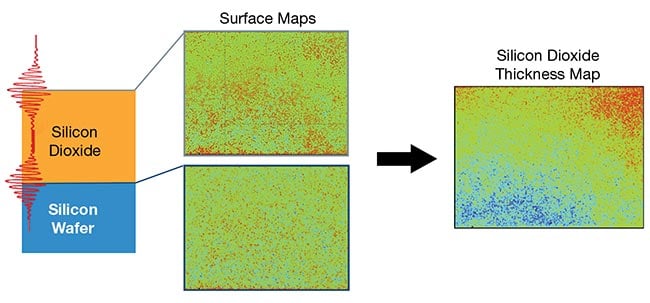
Figure 2. A silicon wafer coated with silicon dioxide, showing fringe envelopes for both material surfaces (left). Surface maps generated from the top of the substrate and the top of the film (middle). When substrate surface value is subtracted from film surface, the resulting value is a thickness map of the silicon dioxide material (right).
Courtesy of Bruker Nano Surfaces and Metrology.
Measurable film thickness is largely determined by objective lens, due to both light penetration and fringe envelope separation. Thicker films require a lower numerical aperture (NA) to allow more vertical light to enter — a feature of lower-magnification lenses. Thin films, meanwhile, require a higher NA to limit depth of focus and improve vertical resolution, thereby avoiding overlapping fringe envelopes. The thinnest films will have overlapping fringe envelopes regardless of objective choice, and these require a dedicated thin-film analysis. Figure 3 shows the interferogram overlap that occurs when a film becomes very thin.
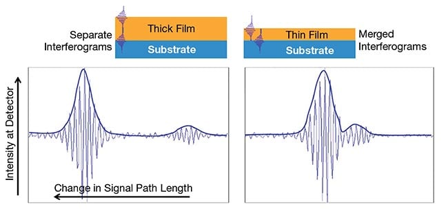
Figure 3. As film thickness decreases, the fringe envelopes from the film surface and substrate surface begin to overlap. Thick-film interferograms show clear separation (left). Thin-film interferograms are merged and are difficult to distinguish without dedicated analysis (right). Courtesy of Bruker Nano Surfaces and Metrology.
Analyzing the thickness of relatively thick films (thickness ≥2 µm) is a straightforward process based on the fringes and separation of fringe envelopes. Upon determining the vertical center of each fringe envelope, distance between the centers is calculated for each camera pixel. Dividing the fringe envelope separation by the film’s index of refraction provides an accurate thickness.
Measuring thin-film (<2-µm) thickness is more complex due to the overlap of the fringe envelopes. Calculations of thin film thickness depend on using an accurate fitting model that can deconvolute the two envelopes. This can be performed using a fringe signal modeling algorithm with a merit function that assesses agreement between the measured data and the built fitting model. Such a fitting model is created by a measurement model from the bare substrate after selecting magnification and film/material calibration models.
Optimizing system selection
Thin-film coatings are found on all kinds of samples, of all shapes and sizes. They exist in all types of environments, from high-throughput manufacturing to small-scale research. Each situation and environment presents distinct challenges for choosing the optimal WLI system.
A key step for determining the appropriate WLI system for a given application is identifying the necessary objective lens(es). This choice requires consideration of the field of view and lateral resolution requirements. Lower-magnification lenses with larger fields of view also mean lower lateral resolution, so it is
essential to understand the priorities of the application. High-throughput semiconductor applications, such as MEMS manufacturing quality control, may require a larger field of view in a single measurement (Figure 4). Alternatively, nanostructure research may prioritize higher magnification for high lateral resolution. No matter the use case, WLI’s sub-angstrom vertical resolution and accuracy are the same at all magnifications.
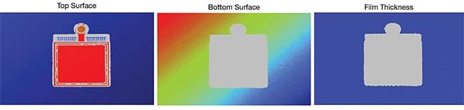
Figure 4. An example of film thickness quality control for microelectromechanical systems (MEMS) manufacturing.
Courtesy of Bruker Nano Surfaces and Metrology.
In ensuring that the selected objective lens for the WLI profiler fits the application needs, it is important to consider that certain interferometric lenses — unlike standard low- and high-magnification lenses — offer specialized features. Sidewall applications will require a mirror attachment to deflect the light beam, whereas deep trenches may require long working-distance lenses. Most objectives are turret mountable, meaning that they allow for one turret to have multiple objectives that cover magnifications from 0.5× to 220×.
Though field of view per scan is defined by objective lens choice, the use of high-quality stitching algorithms can extend the full size of the data array. This enables the user to acquire multiple images and “stitch” them into one resulting image. Using the best stitching algorithms, individual scan frames are indistinguishable in the final height maps. An automated xy stage is required for automated stitching.
The difficulty of focusing on the surface is one traditional challenge to operating a WLI profiler. This becomes a concern and may even become a drawback to WLI in situations in which operator ease of use is essential. Systems that offer automatic focus-finding are a good option in these cases. For these systems, the operator only needs to ensure that the objective is somewhat near focus. The software will then automatically find focal point and optimal illumination settings.
The right system for a given application will also need the necessary measurement modes available to ensure optimal performance. For example, the larger vertical translation of the measurement head in vertical scanning interferometry presents the best approach for tracking rougher surfaces. Meanwhile, phase-shifting interferometry — in which the phase of a monochromatic light beam (often green) is shifted slightly with a piezo to shift the fringe envelope and measure surface height — is typically used to deliver accurate measurements of ultrasmooth surfaces. Surfaces that are somewhere between rough and ultrasmooth, with features of both qualities, are ideally measured using a universal measurement mode. This mode should automatically detect surface texture properties and
appropriately adjust resolution.
Lateral resolution, which is defined by objective choice and the wavelength of the light that is used, can be improved by overcoming the diffraction limit through a combination of hardware and software techniques. Technology now exists to extend a measurement well beyond the diffraction limit, enabling detection of much smaller features. Adding stitching of multiple images into one image further enables high-magnification, high-resolution lateral resolution with large fields of view.
Finally, any combination of unique floor-space, sample, and automation
requirements further dictate the WLI model that is needed for a given use case. Small laboratories limited in space may need to choose a benchtop system. Large samples, such as engine blocks or large lenses, may require a floor-standing system with an open gantry and a high weight limit for the stage. Added high complexity, as in the case of an engine block, could additionally require a tilting head to reposition the objective lens as opposed to the part itself. Available automation levels for ease of use and throughput enhancement range from automated analysis to full automation of the entire measurement, analysis, and reporting process.
Meet the authors
Erica Erickson is a materials science writer who is part of the marketing and communications team at Bruker Nano Surfaces and Metrology. Erickson has a Ph.D. in materials science and engineering; email:
[email protected].
Roger Posusta is a senior marketing application specialist at Bruker Nano Surfaces and Metrology. Posusta has a degree in metrology and more than 35 years of metrology experience in various industries; email:
[email protected].