Full company details
Edinburgh Instruments Ltd.
A Techcomp Instruments Europe Co.
 1 Bain Square
Kirkton Campus
Livingston EH54 7DQ
United Kingdom
Phone: +44 1506 425300
Fax: +44 1506 425320
Photoluminescence Spectroscopy Optimizes Perovskite Quantum Dots
Photonics.com
Sep 2019Perovskite quantum dots could be used to create the next generation of display devices, but first they must be characterized and their emission properties optimized.STUART THOMSON, EDINBURGH INSTRUMENTS
Perovskite semiconductors have attracted tremendous attention in recent years because of the rapid rise of perovskite solar cell efficiencies — from less than 10% to more than 20% in less than five years — and the potential for the materials to provide low-cost solar power
1. The properties that make these materials well suited as absorber layers in solar cells also make them excellent emitters of light, and researchers have shifted their attention toward material optimization for optoelectronic applications such as lasers, lighting, and displays. Of particular interest for display applications are perovskite quantum dots (QDs), which combine the desirable properties of perovskite semiconductors with the excellent control of the light emission offered through quantum confinement (Figure 1).
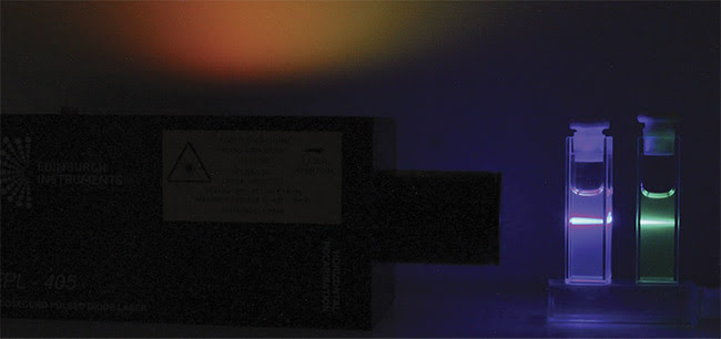
Figure 1. Photoluminescence of perovskite QD solutions when excited using a 405-nm laser.
A perovskite QD is a nanoscale perovskite semiconductor particle that has its optoelectronic properties controlled by quantum confinement effects. In a bulk semiconductor, there are a large number of atoms, and the overlap of this high number of atomic orbitals creates a continuum of closely spaced energy levels that form the valence and conduction bands. By reducing the size of the semiconductor to the nanoscale, this situation changes. Fewer atomic orbitals overlap, the valence and conduction bands are no longer continuous, and — most importantly — the bandgap between the valence and conduction bands becomes wider (Figure 2).
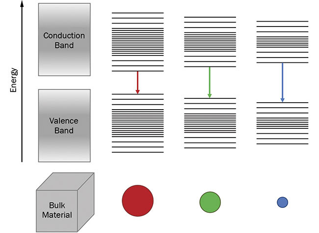
Figure 2. An illustration of the effect of particle size on the bandgap and emission
wavelength caused by quantum confinement. Courtesy of Edinburgh Instruments Ltd.
Quantum confinement dramatically improves the emission properties compared to the bulk semiconductor, with perovskite QDs possessing brighter emission, narrower emission linewidths, and wavelength tunability through particle size control. These desirable properties have caught the attention of researchers developing materials for next-generation displays with wider color gamut, efficien-
cy, and brightness.
Perovskite QDs possess an array of attractive
properties that make them promising candidates
as emitters in next-generation displays.
In standard LED LCD displays available today, a blue LED combined with a phosphor downconversion layer is used to generate broadband white light that is then passed through an RGB color filter to generate the red, green, and blue pixels that make up the display. To create a display with a wide color gamut, the emission linewidth of the red, green, and blue pixels should be narrow. There is a trade-off in doing this, however; narrower linewidths require increased filtering of the white light, which results in more wasted light and reduced brightness and efficiency of the display.
QLED displays
A solution to this problem is to replace the broadband phosphor with a QD downconversion layer to generate the green and red light, which creates one type of so-called QLED display. Because of the intrinsically narrow emission linewidths of QDs, this approach requires less filtering of the light to produce a wide color gamut (Figure 3) and enables displays that simultaneously possess high brightness, high efficiency, and wide color gamut. At present, the cadmium selenide (CdSe) and indium phosphide (InP) families of QDs are used for this purpose. The advantage of perovskite QDs over these mature technologies is that they have considerably narrower emission linewidths (~15 nm versus >30 nm) and therefore require less filtering to achieve the same color gamut.

Figure 3. A simplified illustration of the difference in operation between LED and QLED displays. Courtesy of Edinburgh Instruments Ltd.
Extensive research and development will be required for perovskite QDs to be competitive against these already well-established technologies, with two of the most pressing issues being the poor stability and limited choice of emission wavelengths of currently available perovskite QDs. For perovskite QDs to reach commercialization, new dots with good stability, high brightness, and narrow emission linewidths must be designed, synthesized, and characterized.
During research and development of perovskite QDs, the emission properties of synthesized QDs must be characterized and this information must then be used to refine subsequent designs and syntheses. The most powerful way to characterize the emission properties of these materials is by using photoluminescence spectroscopy. To demonstrate this, a complete photophysical characterization of two perovskite QDs comprising absorption spectra, photoluminescence emission spectra, photoluminescence lifetime, and photoluminescence quantum yield (PLQY) was undertaken using a photoluminescence spectrometer.
The perovskite QDs were first dissolved in cyclohexane, which simulates the fact that the QDs would be dispersed in a polymer host material in a QLED display to prevent concentration quenching. The solutions were diluted until they had an absorbance of 0.1 OD (optical density) at the band edge, which prevented reabsorption errors during the spectral and quantum yield measurements. The solutions were measured using a photoluminescence spectrometer equipped with a 150-W xenon lamp, a photomultiplier tube detector, and a 405-nm picosecond pulsed diode laser.
Absorption and emission spectra
Absorption and emission spectra are the cornerstone of any photophysical characterization, and the spectra of the two perovskite QD solutions, henceforth referred to as PQD-A and PQD-B, were measured (Figures 4a, b).
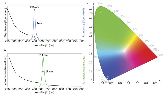
Figure 4. Absorption and photoluminescence properties of perovskite QDs. Absorption and emission spectra of PQD-A (a) and PQD-B (b).
Chromaticity coordinates of the emission (c). Absorption spectra parameters: Δλex = 2 nm. Emission spectra parameters: λex = 350 nm,
Δλex = 1 nm, Δλem = 0.5 nm. Courtesy of Edinburgh Instruments Ltd.
PQD-A is blue emitting, with a central emission wavelength of 450 nm and a full width half maximum (FWHM) of only
14 nm. PQD-B is green emitting with a center wavelength of 514 nm and a similarly narrow FWHM of 17 nm. The narrow emission linewidth of both dots is ideal for creating wide color gamut displays.
Both dots have broad absorption, extending from the ultraviolet down to the band edge of the QD. This broad absorption is another useful property of perovskite QDs, as it enables them to efficiently absorb shorter wavelength photons for downconversion. However, the absorption behavior of the two QDs below the band edge is notably different. The absorbance of PQD-A immediately drops to zero at the band edge, while the absorbance of PQD-B instead decays gradually. This gradual decay in the absorbance is known as an “Urbach tail” and is due to high energetic disorder at the band edge, suggesting that the energetic disorder is higher in PQD-B than PQD-A
2,3,4.
For display applications, it is common to express the emission by its chromaticity coordinates rather than by the peak wavelength. The emission spectra were therefore converted into a chromaticity plot in CIE 1931, the system that takes into account human perception of color and is one of the most commonly used standards for describing color in the display industry (Figure 4c).
Photoluminescence quantum yield
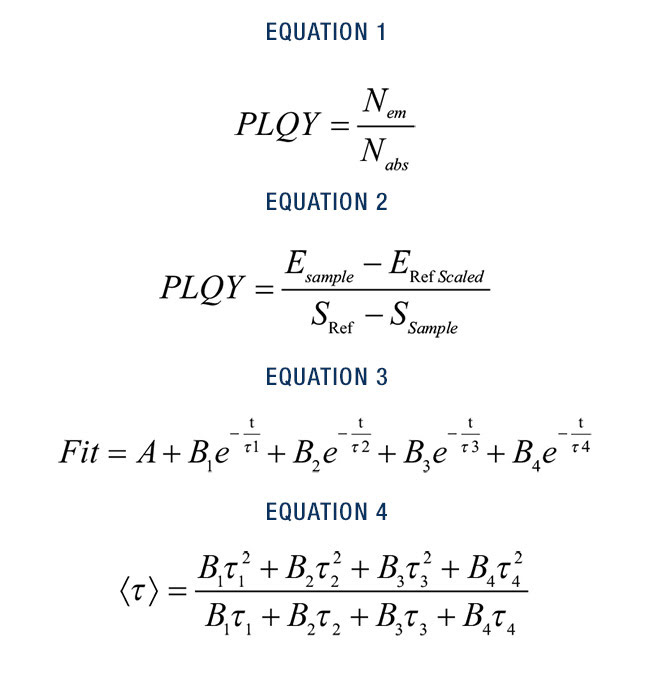
For use in displays, perovskite QDs must have bright emission. The measure of the brightness of emission is called the photoluminescence quantum yield (PLQY) and is the ratio of the photons emitted by a material (Nem) to the photons absorbed (Nabs) (Equation 1).
A PLQY of 100% corresponds to every absorbed photon being reemitted as photoluminescence and is the ideal scenario for a QD emitter. To be used in displays, perovskite QDs will likely require a PLQY in excess of 90%. It is therefore important to measure and optimize the PLQY of newly developed perovskite QDs, and the most accurate method for measuring PLQY is to use an integrating sphere. In an integrating sphere, the sample is optically excited, and all scattered and emitted photons are collected and detected, which enables an absolute determination of the ratio in Equation 1.
To determine the PLQY, the emission and scattering peaks of the reference and sample spectra were integrated and the PLQY was calculated using Equation 2, where S
Sample and S
Ref are the integrated intensities of the scattering peaks of the sample and reference, respectively, E
Sample is the integrated intensity of the sample emission, and E
Ref Scaled is the integrated intensity of the scaled reference emission.
The PLQY of the two dots was found to be 3% for PQD-A and 56% for PQD-B (Figure 5). The high PLQY value of 56% for PQD-B demonstrates the potential of these new emitters. Values of over 90% for similar perovskite QDs have recently been reported in the literature — a yield approaching that achieved by the incumbent CdSe and InP dots
5.
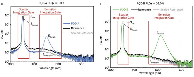
Figure 5. The scattering and emission peaks of the PQD-A (a) and PQD-B (b) solutions are shown in blue and green, respectively. The scattering
and emission integration ranges are shown in red. The scattering and emission peaks of a cyclohexane reference are shown in black and the
scaled reference emission in gray. The scaled reference is used to take into account the higher intensity of scattered light in the sphere when the nonabsorbing cyclohexane reference is present. Experimental parameters: λex = 350 nm, Δλex = 5 nm, Δλem = 0.3 nm. Courtesy of Edinburgh Instruments Ltd.
Photoluminescence lifetime
A final photophysical parameter, which can provide information on performance-limiting loss processes occurring inside the dots themselves, is the photoluminescence lifetime. In a photoluminescence lifetime measurement, the QD solution is excited with a short laser pulse from a picosecond pulsed diode laser, and the photoluminescence decay following the laser pulse is measured using the technique of time-correlated single-photon counting (TCSPC). In TCSPC, the time delay between the laser pulse and the detection of a photoluminescence photon is recorded, and the statistical distribution of these delays is built up photon by photon after each laser pulse to give the photoluminescence decay (Figure 6).
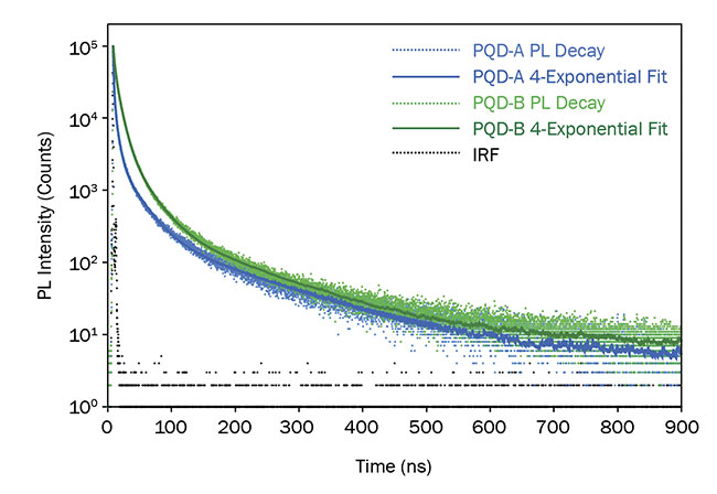
Figure 6. Photoluminescence (PL) decays of PQD-A and PQD-B measured using TCSPC.
Experimental parameters: λex = 405-nm pulsed diode laser, Δλem = 1 nm, λem = 450, 514 nm. IRF: instrument response function. Courtesy of Edinburgh Instruments Ltd.
The photoluminescence decay exhibited by both dots is complex and cannot be fit using a single time constant, which is in agreement with previous literature reports of these materials
5. To extract a photoluminescence lifetime, the decays were fit using reconvolution analysis with a four-component exponential decay (Equation 3) using a reconvolution fitting routine.
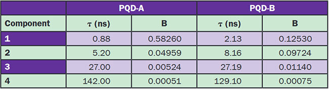
The lifetimes and amplitudes of the four components of the fit are given (Table 1). These four components should not be thought of as distinct physical processes but can instead be used to calculate the average lifetime, <τ>, of the decay using Equation 4. The average lifetimes were found to be 16.1 and 19.1 ns for PQD-A and PQD-B, respectively. The shorter lifetime of PQD-A indicates that there may be more nonradiative recombination in this dot, which could be a contributing factor in its lower PLQY.
Perovskite QDs possess an array of attractive properties that make them promising candidates as emitters in next-generation displays. However, the emission properties of these materials must be further characterized and optimized using photoluminescence spectroscopy. It will be interesting to follow the progress of this burgeoning field and see whether the current problems can be overcome for perovskite QDs to reach commercialization.
Meet the author
Stuart Thomson, Ph.D., is an applications scientist at Edinburgh Instruments. He received his doctorate in semiconductor optoelectronics from the University of St. Andrews and specializes in photoluminescence spectroscopy of semiconductor materials.
References
1. National Renewable Energy Laboratory (NREL) Efficiency Chart, Rev. 01-03-2019.
2. A. Sadhanala et al. (2014). Preparation of single-phase films of CH
3NH
3Pb(I
1−xBr
x)3 with sharp optical band edges.
J Phys Chem Lett, Vol. 4, pp. 2501-2505.
3. H. He et al. (2016). Exciton localization in solution-processed organolead trihalide perovskites.
Nat Commun, Vol. 7, p. 10896.
4. B. Wenger et al. (2017). Consolidation of the optoelectronic properties of CH
3NH
3PbBr
3 perovskite single crystals.
Nat Commun, Vol. 8, p. 590.
5. X. Li et al. (2016). CsPbX3 quantum dots for lighting and displays: room temperature, synthesis, photoluminescence superiorities, underlying origins and white light-emitting diodes.
Adv Func Mater, Vol. 26, pp. 2435-2445.