Full company details
SCANLAB GmbH
 Siemensstr. 2a
82178 Puchheim
Germany
Phone: +49 89 800746 0
Fax: +49 89 800746 199
Accelerating the Manufacture and Repair of Micro-LED Displays
Photonics Spectra
Dec 2021A novel laser-scanning setup introduces a precise and more rapid approach to the laser-induced forward transfer repair process for micro-LED display manufacture.THOMAS MANN AND HOLGER SCHLÜTER, SCANLAB GMBH
While LCD panels are passive displays that need backlight illumination, OLEDs and LEDs are active elements that eliminate the need for backlighting by emitting their own light. OLEDs have their own drawbacks compared to LEDs, most notably the burn-in effect, which limits their display life. Of all these options, micro-LEDs — which are miniaturized LEDs in a display matrix — offer the most numerous advantages for display applications
1, including:
Courtesy of iStock.com/CharnW.
• Higher luminous efficiency, brightness, and contrast.
• Wider viewing angles.
• Higher resolutions due to greater pixel density.
• Longer lifetimes, with improved reliability and environmental stability.
• Faster refresh rates, with response times in the nanoseconds.
• Absence of backlight, which allows thinner and lighter displays with lower power consumption.
Micro-LEDs, however, are not without their own challenges, and high-volume manufacturing of these displays is among them. Consequently, current micro-LED displays have a large pixel size when compared to what is achievable with LCD and OLED displays. Samsung, for example, recently introduced a micro-LED display called The Wall that has a pixel pitch of 0.8 mm. The display is fabricated using mechanical pick-and-place manufacturing techniques. Modern cellphone displays need a much smaller pitch of 0.03 to 0.06 mm and 400 to 800 pixels per inch (PPI). So, for example, micro-LED sizes of 35 × 20 sq µm are necessary to satisfy display manufacturers’ needs.
Currently, the accuracy of pick and place is not suitable for such small die sizes. Therefore, new laser-based techniques are required for the transfer of the dies. Also, upscaling display fabrication for the mass market requires a significant increase in throughput that mechanical techniques cannot meet. Laser-assisted technologies prove to be the only capable alternative that satisfies these demands and aligns with the various processes involved in the multistep manufacturing of micro-LED displays with high PPI densities.
Manufacturing micro-LED displays
The laser is a fundamental tool in the mass manufacture of micro-LED displays. Individually colored red, green, and blue (RGB) micro-LEDs, typically based on the inorganic III-V semiconductor gallium nitride (GaN), are first grown on individual epiwafers, commonly sapphire, at an approximate density of 8 million per 6-in. wafer, as shown on the left side of Figure 1.
The task is then to transfer and interlace these differently colored micro-LEDs onto a substrate with higher thermal and electrical conductivity to form a color display. This encompasses various laser-based processes, as shown on the right side of Figure 1.
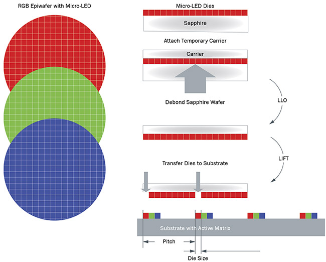
Figure 1. The laser processes used during the mass-manufacturing of micro-LEDs. LLO: laser lift off; LIFT: laser-induced forward transfer. Courtesy of Coherent.
Initially, a temporary carrier is attached to the micro-LED before the sapphire wafer is debonded using the laser lift-off (LLO) technique. A high throughput scan strategy uses xy stages to move the substrate under a laser line that spans the length of the wafer with a top-hat intensity profile to produce a uniform material interaction.
It is necessary to employ a wavelength in the UV spectrum below the 3.3-eV (376-nm) bandgap of GaN but above the 9.9-eV (125-nm) bandgap of sapphire, where the sapphire substrate is transparent and the LEDs are opaque. Pulsed UV lasers, such as 248-nm excimers or 266-nm picosecond lasers, are capable of limiting the interaction volume to a few nanometers, therefore minimizing stress on the device layer
2.
After preparing the micro-LEDs on the temporary carrier, the laser-induced forward transfer (LIFT) method, based on a mask technique with modern excimer lasers, enables their selective transfer and RGB arrangement on the final display substrate. To mass-transfer the micro-LEDs, illuminating a mask with a large top-hat beam profile provides uniform force to achieve an individual positioning accuracy of a few microns
2.
Depending on the pitch and the specific process condition, it is possible to transfer up to 10,000 dies per shot. With modern excimer lasers’ repetition rates of a few 100 Hz, this equates to a few million dies per second and a processing time of tens of seconds for a 6-in. wafer. Due to the one-shot interaction and large illumination area, a laser with excellent pulse-to-pulse stability and high pulse energy is necessary.
Manufacturing bottlenecks remain: Even with the highest yields, the mass-transfer process results in several thousand dead pixels per wafer. Each of these pixels must be replaced, which requires development of fast and individual addressable processes.
These processes impose the same demand for beam quality and high throughput as the fabrication step.
Solid-state ultrashort-pulse lasers operating in the kilohertz range, in combination with scanning techniques, present a capable and cost-efficient solution. Higher repetition rates also require careful consideration of scanning techniques because the xy stages cannot provide the required accelerations.
Micro-LED repair
To ensure accurate and precise processing, the intensity profile of the focused laser beam at each micro-LED repair site must be well defined across the entire wafer. Specifically, the profile should
exhibit a small rectangular shape with steep edges of 3 to 5 µm and a uniform flat region. This is achievable by using a short focal length f-theta lens together with a custom sharp-edge top-hat beam shaper. Such diffractive optical elements (DOEs) provide a top-hat intensity profile with a flat region size only a few times larger than the diffraction-limited spot and an improved sharp edge with a width of half the diffraction-limited spot.
A sharp-edge top-hat profile that satisfies these conditions appears in Figure 2
and was achieved using a HOLO/OR beam-shaper DOE in combination with
an f-theta lens (f = 65.5 mm) to focus
the Gaussian beam of a 355-nm laser (Coherent HyperRapid 50 classic) and a SCANLAB excelliSCAN 14 galvo scanner. A highly accurate beam size, good centration of the beam, and precise focusing are critical for optimal performance.
This performance is achievable using a module from Pulsar Photonics with automated-measurement routines and
actuators that automatically align the laser beam to the top-hat shaper and
calibrate the system. The automatic alignment ensures a stable calibration over longer processing times.
The challenge of laser scanning with a shaped beam is that distortion increasingly occurs toward the edges of the image field, as shown in Figure 3a. This distortion is due to the barrel-pillow-shaped image field that results from the arrangement of the galvo mirrors and the imaging properties of the f-theta lens
3.
Other effects, such as clipping of higher diffraction orders and the introduction of wavefront errors by the optics in the beam path, can also play a role.
For the top-hat beam profile shown in Figure 2, only the central region of the entire 16- × 16-sq-mm image field was scannable before a decrease in uniformity and a deformation of the shape occurred at a level not suitable for micro-LED processing.
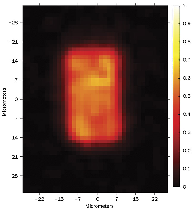
Figure 2. A top-hat profile for which only the central region of a 16- × 16-sq-mm image field was scannable before a lack of uniformity in intensity made processing micro-LEDs difficult. The challenge of laser scanning with a shaped beam is that distortion often occurs toward the edges of the image field. Effects that underly this phenomenon include the clipping of higher diffraction orders and the introduction of wavefront errors
by the optics in the beam path. Courtesy of Pulsar Photonics/SCANLAB.
To overcome this limitation, it is necessary to use an xy stage to raster the wafer during processing, as in Figure 3b.
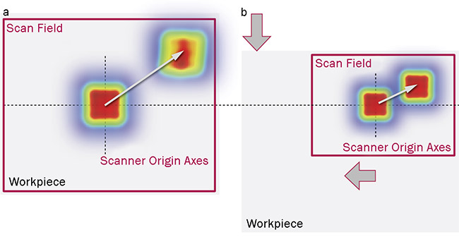
Figure 3. During laser scanning with a top-hat-shaped beam profile, warping occurs at the image field’s extremities due to increased aberrations (a). This distortion can be compensated for by leveraging the
synchronous motion of an xy stage during processing to limit the scan field size to the central field of view
of the f-theta lens (b). Courtesy of Pulsar Photonics/SCANLAB.
For high process speeds, the stage and scanner motion can be synchronized using an innovative solution developed
by SCANLAB and ACS Motion Control. A special algorithm within the control
software generates synchronized
trajectories for the scanner and stage, respectively. This joint motion strategy
eliminates the stitching errors and improvements in accuracy that are more typical of stitch-and-scan or marking-
on-the-fly strategies.
Figure 4 shows a 4-sigma (99.99% of shots) absolute positioning error of just 2.82 µm when using this method to process 10,000 points with a 6- × 6-sq-mm scan field and a 100-µm pitch at 2.6 kHz (and a jump delay of 40 µs and a 150-µs processing time)
4.
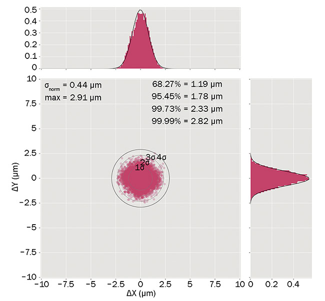
Figure 4. A 2D scatter plot of the positioning error with a setup that combines a scanning system outfitted with an f = 100 mm f-theta lens and a mechanical stage moving in synchronized motion. Density plots along the x and y axes are shown separately and exhibit a Gaussian distribution. Courtesy of Pulsar Photonics/SCANLAB.
Figure 5 shows the scanning strategy of a 5- × 5-sq-mm field of view over the wafer, as described. Processing a 6-in. wafer is achievable in a matter of seconds, satisfying industry throughput demands. In principle, this enables the processing of wafers with diameters up to the travel range of the stages. In practice, however, 8 in. is the current upper limit for micro-LED displays due to their high flatness and layer homogeneity requirements.
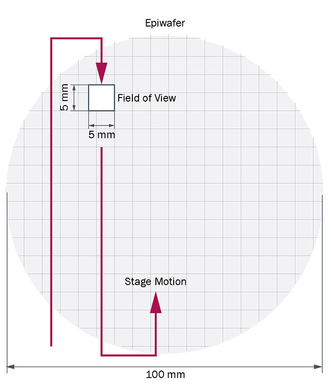
Figure 5. To achieve high throughput during micro-LED repair processes, the scan field can be limited to the central 5- × 5-sq-mm field of view of the f-theta lens. This ensures good imaging performance of the laser’s top-hat intensity profile, while the stage motion allows the entire epiwafer to be processed. Courtesy of SCANLAB.
Micro-LEDs offer a promising new
display technology with significant
advantages over LCDs and OLED displays. But they also require demanding manufacturing technologies that currently remain under development. Laser processes are at the core of these manufacturing technologies.
A combination of the LLO and LIFT techniques is necessary for mass-transfer of micro-LEDs, and this involves the use of a mask-based excimer laser process. Illuminating a mask with a large top-hat beam profile provides uniform force to achieve an individual positioning accuracy of a few microns. However, during manufacturing, several thousand dies are typically defective and need to be replaced. Using a UV picosecond laser can satisfy the requirements of this repair process and achieve high throughput. Essentially, a scanning technology based on low-distortion, top-hat beam shaping, in combination with the scanning strategy presented here, looks to be a promising solution.
Meet the authors
Thomas Mann, Ph.D., has been working as a technical sales engineer at SCANLAB GmbH since 2020. He earned his doctorate in ultrafast laser-matter interactions at the University of Leeds in England. After working in previous roles developing photonic devices, he now specializes in the development and distribution of highly integrated scan systems with diffractive optics for high-precision applications; email:
[email protected].
Holger Schlüter, Ph.D., received his doctorate in physics at the Insitut Lasertechnik in Aachen, Germany. Between 1996 and 2008 he worked for TRUMPF in various positions in Germany and in the U.S. He was CTO and COO at Technolas Perfect Vision in Germany and general manager of HIGHYAG. For the past six years, he has been the head of business development for SCANLAB GmbH; email:
[email protected].
References
1. RF Wireless World. Advantages of micro LED, disadvantages of micro LED,
www.rfwireless-world.com/terminology/advantages-and-disadvantages-of-micro-led.html.
2. B. Zhang and O. Haupt (2021). MicroLED: high throughput laser based mass transfer technology.
Proc ICDT, Vol. 52, Issue 52, Beijing.
3. P. Verboven (1988). Distortion correction formulas for pre-objective dual galvanometer laser scanning.
Appl Opt, Vol. 27,
No. 20, pp. 4172-4173.
4. H. Schlüter and S. Eifel (2021). Variable multibeam tool enables high accuracy and throughput.
Laser Focus World, Vol. 57,
No. 5, pp. 29-32.