|
Thursday, November 14, 2019 |
|

|
|
|

|
| sponsor |
 |
|
AI Improves Quality and Usability of Optoacoustic Imaging
To improve image quality in low-cost optoacoustic devices with only a small number of ultrasonic sensors, researchers at ETH Zurich and the University of Zurich developed a framework for the efficient recovery of image quality from sparse optoacoustic data using a deep convolutional neural network and demonstrated their approach with whole body mouse imaging in vivo.
|
|
|
|
|
|
Bioinspired Sensor Uses Metalenses for Depth from Defocus
Researchers at the Harvard John A. Paulson School of Engineering and Applied Sciences (SEAS) have developed a compact sensor that can measure depth in a single shot. The sensor’s design was inspired by the specialized optics of the jumping spider.
|
|
|
|
|
|
Improved Holographic Printing Technology Creates Realistic Colorful Holograms
Researchers have developed a printer that is able to produce digital 3D holograms with an unprecedented level of detail and realistic color. The printer could be used to create high-resolution color re-creations of objects or scenes for museum displays, architectural models, fine art, or advertisements that do not require glasses or special viewing aids.
|
|
|
|
|
|
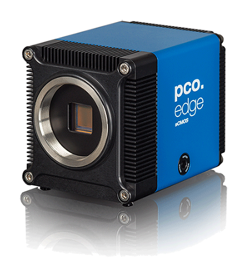 pco.edge 26 sCMOS Camera
PCO-TECH Inc.
Maximizing the amount of information per image is crucial for microscopy, quality control, high throughput screening, and other mesoscopic applications. This is where the new pco.edge 26 fits superb. The pco.edge 26 offers you a 5120 x 5120 pixel resolution with 2.5 x 2.5 µm² pixel size.
Visit Website
Request Info
|
|
|
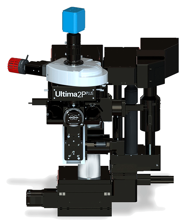 Ultima 2Pplus Multiphoton Imaging
Bruker Nano Surfaces
With new advances in field of view, sensitivity, wavelength, and sample accommodation, Bruker’s Ultima 2Pplus delivers the best commercially available combination of flexibility, resolution, imaging depth, and speed, allowing users to perform simultaneous imaging, stimulation, and electrophysiology protocols with greater efficiency and effectivity.
Visit Website
Request Info
|
|
|
|
|
|
Researchers Engineer Light-Activated Cells for Treating Diabetes
Tufts University researchers have shown that glucose levels can be controlled in a mouse model of diabetes through optogenetics. When exposed to light, engineered pancreatic beta cells transplanted into diabetic mice produced more than two to three times the typical level of insulin.
|
|
|
|
|
|
Light-Based 'Tractor Beam' for Nanoscale Assembly
Researchers from the University of Washington have developed a method that could make reproducible manufacturing at the nanoscale possible. The team adapted an existing technique pioneered by Arthur Ashkin, optical tweezers, to operate in a water-free liquid environment of carbon-rich organic solvents.
|
|
|
|
|
|
Empire State Development Announces Round III Finalists of the Luminate NY Accelerator Read Article
Commemorating 30 Years of Optical Vortices Read Article
ZEISS and Kyoto University Sign Research Agreement Read Article
Transparent Displays Become More Affordable, Flexible Read Article
Satellites Could Help Quantify, Monitor Ocean Carbon Read Article
|
|
|
|
Semicon Japan 2019
December 11-13, 2019 - Tokyo Big Sight, Tokyo, Japan - Tokyo
Japan supplies one-third of all semiconductor equipment and more than one-half of all materials to the global semiconductor manufacturing industry. SEMICON Japan takes place in the heart of the semiconductor supply chain with more than 700 exhibiting companies from Japan and other regions, showcasing innovative solutions for your technology challenges and business success. Workplaces are increasingly driven by automation, and this is creating more opportunities for exponential growth in chip manufacturing. Make the most of these opportunities at SEMICON Japan 2019. Deepen your connections with the Japan and global electronics manufacturing supply chain.
|
|
|
|
Frequency-Domain Fluorescence Lifetime Imaging System Improvements and Applications
Wed, Nov 20, 2019 10:00 AM - 11:00 AM EST
Since its introduction in 2014, the FD-FLIM pco.flim camera system has been applied to many different areas, from FRET to endogenous fluorescence, from oxygen to pH measurement, from large technical applications to light-sheet microscopy. In this webinar presented by PCO, Gerhard Holst will demonstrate and discuss improvements in the use and applicability of the pco.flim camera. New results including investigation of microplastics on lab filters, pH measurements, oxygen measurements in a marine environment, assistance for neurosurgery, and rapid FD-FLIM measurements will be shown to demonstrate the flexibility of the pco.flim camera system.
|
|
|
|
3D Microprinting: How Small Can We Go?
Tue, Nov 19, 2019 10:00 AM - 11:00 AM EST
High-resolution and submicron precision are key requirements for producing 3D polymer structures at microscale for use in industrial applications. In this webinar you will learn about two-photon polymerization (2PP), a technology that enables 3D-printing resolution as small as 0.2 µm. The presenter will provide examples of applications in different fields, such as micro-optics, microfluidics, metamaterials, and scaffold for tissue engineering.
|
|
|
|

CALL FOR ARTICLES
Photonics Media is currently seeking technical feature articles on a variety of topics for publication in our magazines (Photonics Spectra, BioPhotonics, Vision Spectra, and EuroPhotonics). Please submit an informal 100-word abstract to [email protected], or use our online submission form.
|
|
|
|
 |
|