2D Material Growth Process
Oxford Instruments PLC, Magnetic Resonance, NanoScienceRequest Info
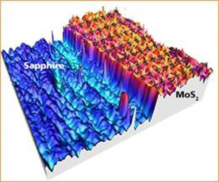
 Oxford Instruments plc has announced MoS2 growth process using the Nanofab nanoscale growth system.
Single-layer MoS2 is a direct band gap semiconductor with wide ranging applications in optoelectronics such as LEDs, photovoltaics, photodetectors and biosensors, while multilayer MoS2 is an indirect band gap semiconductor for digital electronics.
The process was developed on a Nanofab system equipped with precursor delivery modules capable of delivering a wide range of liquid, solid and metal organic precursors suitable for 2D materials growth. Offering growth on a range of substrates including sapphire and atomic layer deposition alumina, the system is capable of depositing other 2D transition metal dichalcogenides.
https://www.oxinst.com
/Buyers_Guide/Oxford_Instruments_PLC_Magnetic_Resonance/c11302
Published: July 2016
REQUEST INFO ABOUT THIS PRODUCT
* First Name:
* Last Name:
* Email Address:
* Company:
* Country:
Message:
When you click "Send Request", we will record and send your personal contact information to Oxford Instruments PLC, Magnetic Resonance, NanoScience by email so they may respond directly. You also agree that Photonics Media may contact you with information related to this inquiry, and that you have read and accept our
Privacy Policy and
Terms and Conditions of Use.
Register or login to auto-populate this form:
Login
Register
* Required