Automated Metrology System
EV Group (EVG)Request Info
ST. FLORIAN, Austria, July 13, 2016 — 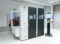 EV Group has announced the EVG 50 automated metrology system, designed to support stringent manufacturing requirements for advanced packaging, MEMS and photonics applications.
The EVG 50 performs high-resolution, nondestructive, multilayer thickness and topography measurement, as well as void detection, in bonded wafer stacks and photoresists used in optical lithography.
The system measures layers down to 2 μm in thickness, inspects up to 1 million points and achieves throughputs of up to 55 300-mm wafers/hour. This combination of extremely high resolution and high throughput provides cost-efficient full-wafer inspection that enables device manufacturers to improve their wafer bonding and lithography processes, as well as achieve higher yields.
https://www.evgroup.com
/Buyers_Guide/EV_Group_EVG/c4622
Published: July 2016
REQUEST INFO ABOUT THIS PRODUCT
* First Name:
* Last Name:
* Email Address:
* Company:
* Country:
Message:
When you click "Send Request", we will record and send your personal contact information to EV Group (EVG) by email so they may respond directly. You also agree that Photonics Media may contact you with information related to this inquiry, and that you have read and accept our
Privacy Policy and
Terms and Conditions of Use.
Register or login to auto-populate this form:
Login
Register
* Required