Circuit/Chip Packaging Platform
Advanced Semiconductor Engineering Inc. (ASE)Request Info
SUNNYVALE, Calif., June 20, 2022 — 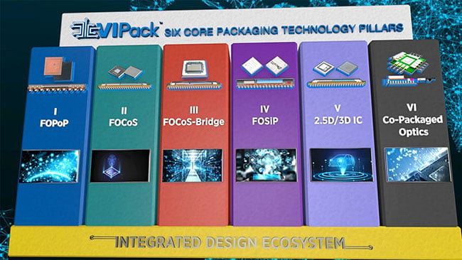 The VIPack™ packaging platform from Advanced Semiconductor Engineering Inc. is designed to enable vertically integrated package solutions.
The platform leverages advanced redistribution layer processes, embedded integration, and 2.5D and 3D technologies when integrating multiple chips within a single package. The six core packaging technology pillars include high-density, RDL-based Fanout Package-on Package (FOPoP); Fanout Chip-on-Substrate, (FOCoS); Fanout Chip-on-Substrate-Bridge (FOCoS-Bridge); Fanout System-in-Package (FOSiP); and Through Silicon Via (TSV)-based 2.5D, 3D integrated circuit and co-packaged optics processing capabilities.
https://ase.aseglobal.com
/Buyers_Guide/Advanced_Semiconductor_Engineering_Inc_ASE/c33233
Published: June 2022
REQUEST INFO ABOUT THIS PRODUCT
* First Name:
* Last Name:
* Email Address:
* Company:
* Country:
Message:
When you click "Send Request", we will record and send your personal contact information to Advanced Semiconductor Engineering Inc. (ASE) by email so they may respond directly. You also agree that Photonics Media may contact you with information related to this inquiry, and that you have read and accept our
Privacy Policy and
Terms and Conditions of Use.
Register or login to auto-populate this form:
Login
Register
* Required