3-D Optical Microscope
Bruker Nano SurfacesRequest Info
Bruker Corp. has launched the ContourSP, a large-panel 3-D metrology system for gauging individual layers of printed circuit board (PCB) panels during manufacturing.
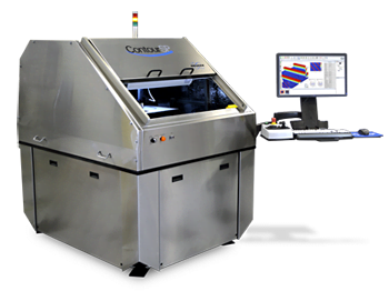 Based on white-light interferometry, the technology is designed to enable minimum recipe development time, maximum uptime, and increased measurement throughput of high-density interconnect substrates in multichip modules.
The system features the proprietary Vision64 operating and analysis software.
https://www.bruker.com/nano
/Buyers_Guide/Bruker_Nano_Surfaces/c19385
Published: December 2013
REQUEST INFO ABOUT THIS PRODUCT
* First Name:
* Last Name:
* Email Address:
* Company:
* Country:
Message:
When you click "Send Request", we will record and send your personal contact information to Bruker Nano Surfaces by email so they may respond directly. You also agree that Photonics Media may contact you with information related to this inquiry, and that you have read and accept our
Privacy Policy and
Terms and Conditions of Use.
Register or login to auto-populate this form:
Login
Register
* Required