Custom Patterned Optics
Reynard CorporationRequest Info
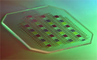
 Reynard Corp. has begun offering custom photolithography services to manufacture patterned optics with geometries as small as 5 μm on substrates up to 18 in. in diameter.
The process involves a contact exposing technique and a variety of thin-film coating. Metallic or dielectric materials can be selected based on the application’s transparent, reflective and conductive optoelectronic requirements. Patterns can be applied to most substrate materials, including plastic sheeting.
Patterned optics applications include eliminating electromagnetic interference (EMI) for sensitive metal-coated electro-optical systems, heated windows, wideband beamsplitters, encoder disks, LCDs, bar codes, reticles, transducers and precision reference targets.
https://reynardcorp.com
/Buyers_Guide/Reynard_Corporation/c12736
Published: March 2015
REQUEST INFO ABOUT THIS PRODUCT
* First Name:
* Last Name:
* Email Address:
* Company:
* Country:
Message:
When you click "Send Request", we will record and send your personal contact information to Reynard Corporation by email so they may respond directly. You also agree that Photonics Media may contact you with information related to this inquiry, and that you have read and accept our
Privacy Policy and
Terms and Conditions of Use.
Register or login to auto-populate this form:
Login
Register
* Required