
Direct-Write E-Beam System
JEOL USA Inc.Request Info
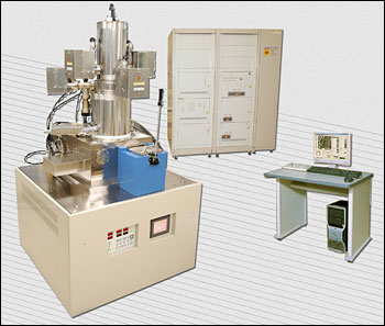
JEOL USA's new high resolution direct-write e-beam lithography system complements its line of spot beam, vector scan systems and mask production tools.
The new JBX-5500FS direct-write lithography tool writes patterns at a minimum linewidth of 10 nm at 50 kV on up to 100-mm substrates. The PC-controlled operating platform features a simple graphical user interface for pattern design and machine control.
 "We are especially pleased to be able to offer this new lithography product during our 40th anniversary since the introduction of the first JEOL e-beam system," said Zane Marek, JEOL USA semiconductor equipment product manager. "JEOL prides itself on having the widest range of tools in its e-beam family of both direct-write and mask production systems," he said.
The company introduced a next-generation direct-write tool, the JBX-6300FS, for sub-10 nm linewidths at 100 kV with sub-15 nm stitching accuracy, in 2006. The first US installation of the JBX-6300FS was completed last month and the second will be completed in August, the company said.
The JBX-6300FS is capable of writing minimum linewidths of 8 nm on 2-in. to 200-mm wafers in either nanolithography or high throughput mode. The JBX-9300FS, JEOL’s production-level e-beam system, handles up to 300-mm wafers.
"The new direct-write tool (JBX-5500FS) would be an ideal choice for research labs or universities. For the past several years, there has been a void between the two most common direct-write tools -- SEMs, or scanning electron microscopes with e-beam attachments, and dedicated e-beam systems. The price gap between these levels has been too large to overcome, especially for universities," Marek said.
For more information, visit: www.jeolusa.com; e-mail: [email protected]JEOL USA Inc.
11 Dearborn Rd.
Peabody, MA 01960
Phone: (978) 535-5900
Fax: (978) 536-2205
https://www.jeolusa.com
/Buyers_Guide/JEOL_USA_Inc/c7365
Published: July 2007
REQUEST INFO ABOUT THIS PRODUCT
* First Name:
* Last Name:
* Email Address:
* Company:
* Country:
Message:
When you click "Send Request", we will record and send your personal contact information to JEOL USA Inc. by email so they may respond directly. You also agree that Photonics Media may contact you with information related to this inquiry, and that you have read and accept our
Privacy Policy and
Terms and Conditions of Use.
Register or login to auto-populate this form:
Login
Register
* Required