
FIB-SEM Workstation
Carl Zeiss Microscopy GmbH, Electron- and Ion-Beam MicroscopesRequest Info
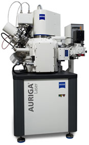
Carl Zeiss’ Auriga laser system combines the advantages of its Auriga CrossBeam focused ion beam/scanning electron microscope (FIB-SEM) workstation with the capabilities of a pulsed microfocus laser for fast ablation of materials.
The laser is useful for examining samples where the target structure is buried under material layers that must be removed — a procedure difficult to conduct with conventional techniques. Mechanical ablation and cross-sectioning of large material volumes often cause deformations, making the sample unsuitable for further examination, and applying a focused ion beam is inefficient because the process is too slow.
 Performing ablation with a pulsed microfocus laser beam does not damage the sample and enables ablation rates comparable to those achieved by mechanical removal.
The scanning laser is a Trumpf AG nanosecond pulsed diode-pumped solid-state laser operating at 355 nm. It was chosen to meet the demands of preparing structures for SEM examination. In cooperation with Carl Zeiss, researchers from Fraunhofer-Institute for Nondestructive Testing have optimized the work flow of the tool for ease of use, fast transfer procedures and fast relocation of the region of interest on the sample under examination.
To protect the workstation and detectors from debris generated during laser ablation, the system is equipped with a separate chamber for laser operation. After the structure of interest is prepared with the laser, the sample is transferred under vacuum conditions to the main chamber for SEM examination or FIB polishing. The target structure is retrieved automatically. The transfer is carried out quickly and smoothly in seconds, resulting in simple and continuous work flow. To realize specific ablation patterns, the laser is equipped with CAD software that controls the scanner head, enabling the user to predefine even highly complex patterns of the sample structure.
The system enables the user to examine complex structures such as next-generation nanotechnology processors and flexible thin-film solar cells.
Applications include semiconductor manufacturing, photovoltaics, polymer electronics, pharmaceuticals, life sciences and materials research. The system is also suitable for the preparation of microsystems that contain soft or brittle phases, such as foams, lightweight construction materials, glass fibers and ceramics, composite materials, pore filters and geological samples.
http://www.zeiss.com/microscopy
/Buyers_Guide/Carl_Zeiss_Microscopy_GmbH_Electron-_and/c20191
Published: March 2012
REQUEST INFO ABOUT THIS PRODUCT
* First Name:
* Last Name:
* Email Address:
* Company:
* Country:
Message:
When you click "Send Request", we will record and send your personal contact information to Carl Zeiss Microscopy GmbH, Electron- and Ion-Beam Microscopes by email so they may respond directly. You also agree that Photonics Media may contact you with information related to this inquiry, and that you have read and accept our
Privacy Policy and
Terms and Conditions of Use.
Register or login to auto-populate this form:
Login
Register
* Required