
Helios NanoLab 1200AT Analysis System
FEI Life Sciences (acquired by Thermo Fisher)
FEI’s new Helios NanoLab 1200AT full-wafer DualBeam analysis system includes an optional automated front-opening universal pod loader, which allows location of the system inside the semiconductor wafer fab. Here, its scanning electron microscope imaging and precise focused ion beam milling are used to extract ultrathin samples of targeted structures and defects for examination in a high-resolution transmission electron microscope (TEM).
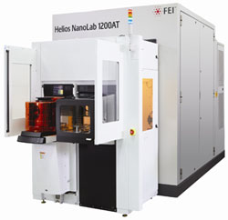 The results are used to diagnose the root cause of a defect and evaluate process maturity. Moving the system closer to the wafer process line can deliver this information up to three times faster than laboratory-based analysis of cleaved wafer pieces. The system can also create site-specific TEM samples thin enough to capture a single transistor at the 10-nm node, from wafers up to 300 mm in diameter.
The company’s iFast automation software combines wafer-, defect- and cell-level navigation with recipe definition and execution in a single program. The integrated EasyLift micromanipulator and QuickFlip grid holders support the creation of ultrathin TEM samples. The MultiChem gas delivery system allows precise control of beam chemistry for fast, selective etching and deposition of protective coatings. An optional low-kV STEM detector provides improved materials contrast, which allows full defect root cause analysis within the fab on a single system.
https://www.fei.com/life-sciences
/Buyers_Guide/FEI_Life_Sciences_acquired_by_Thermo_Fisher/c20082
Published: June 2013