In-House Wafer Testing
SenseekerRequest Info
SANTA BARBARA, Calif., Aug. 12, 2020 — 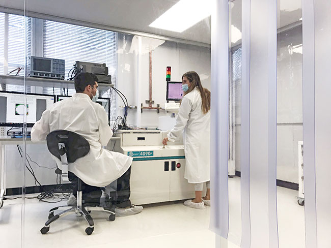 In-house wafer testing from Senseeker Engineering Inc. provides a cleanroom-based wafer probe, supporting quick-turn results.
The facility is equipped to perform testing on items ranging from semiconductor die to assembled integrated circuits under an extreme range of conditions including cryogenic and high-temperature oven testing. In addition to reducing wafer delivery cycle times, Senseeker is equipped to support specialized customer test, failure analysis, and manufacturing yield enhancements.
The Electroglas 4090u wafer prober provides fully-automated, state-of-the-art die probing capability in a Class 10,000 clean room environment.
https://www.senseeker.com
/Buyers_Guide/Senseeker/c32403
Published: August 2020
REQUEST INFO ABOUT THIS PRODUCT
* First Name:
* Last Name:
* Email Address:
* Company:
* Country:
Message:
When you click "Send Request", we will record and send your personal contact information to Senseeker by email so they may respond directly. You also agree that Photonics Media may contact you with information related to this inquiry, and that you have read and accept our
Privacy Policy and
Terms and Conditions of Use.
Register or login to auto-populate this form:
Login
Register
* Required