Integrated Circuit Multiproject Wafer Process
CEA-LetiRequest Info
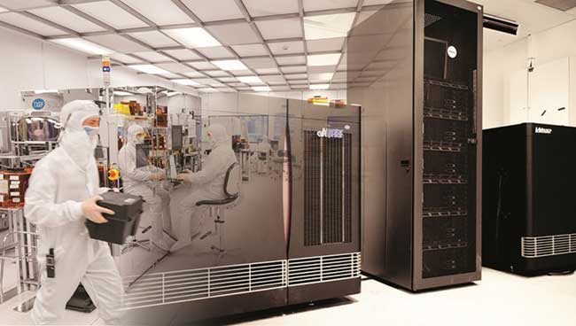
 Leti has announced a multiproject-wafer (MPW) process for the integrated-circuit industry, fabricating emerging nonvolatile memory OxRAM (oxide-based resistive RAM) devices on a 200-mm foundry base-wafer platform.
Available on Leti’s 200mm CMOS line, the MPW service provides a comprehensive, low-cost way to explore techniques designed to achieve miniaturized, high-density components. Including Leti’s Memory Advanced Demonstrator (MAD) future mask set with disruptive OxRAM technology, Leti’s integrated silicon memory platform is developed for backend memories and nonvolatility associated with embedded designs. The new technology platform will be based on titanium-doped hafnium oxide active layers.
Emerging OxRAM nonvolatile memory can be implemented in classical embedded memory applications on advanced nodes like microcontrollers or secure products, as well as for artificial intelligence accelerators and neuromorphic computing.
https://www.leti-cea.com
/Buyers_Guide/CEA-Leti/c24495
Published: September 2018
REQUEST INFO ABOUT THIS PRODUCT
* First Name:
* Last Name:
* Email Address:
* Company:
* Country:
Message:
When you click "Send Request", we will record and send your personal contact information to CEA-Leti by email so they may respond directly. You also agree that Photonics Media may contact you with information related to this inquiry, and that you have read and accept our
Privacy Policy and
Terms and Conditions of Use.
Register or login to auto-populate this form:
Login
Register
* Required