Laser Ablation Processing
TESCANRequest Info
BRNO, Czech Republic, Nov. 3, 2021 — 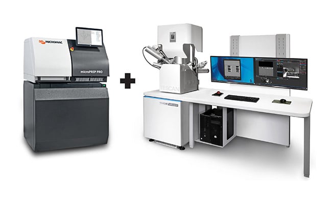 The Large Volume Workflow from TESCAN Orsay Holding AS provides fast failure and defect root-cause analysis in semiconductor manufacturing and materials research.
The method implements correlative microscopy techniques to provide parallel processing through standalone laser ablation and plasma focused ion beam systems. The laser ablation system can prepare samples for multiple downstream tools, resulting in an increase in analytical throughput and productivity to reduce cost per analysis. Rapid cubic-millimeter-scale material removal is provided for sample preparation and analysis workflows, harnessing fast material removal rates, even for nonconductive hard materials like glass and ceramics.
https://www.tescan.com
/Buyers_Guide/TESCAN/c22249
Published: November 2021
REQUEST INFO ABOUT THIS PRODUCT
* First Name:
* Last Name:
* Email Address:
* Company:
* Country:
Message:
When you click "Send Request", we will record and send your personal contact information to TESCAN by email so they may respond directly. You also agree that Photonics Media may contact you with information related to this inquiry, and that you have read and accept our
Privacy Policy and
Terms and Conditions of Use.
Register or login to auto-populate this form:
Login
Register
* Required