LumiMap Electroluminescence System
Bruker Nano SurfacesRequest Info
Bruker Corp. has introduced the LumiMap electroluminescence system for optical and electrical characterization on epitaxial (epi) growth wafers for high-brightness (HB) LEDs.
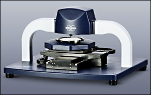 An alternative to conventional indium dot methods of epi wafer characterization, the system features nondestructive measurement requiring no chemical cleaning afterward; software-controlled measurement locations; and repeatable optical and electrical measurement capabilities through forming a temporary LED device on an epi wafer. The results correlated with those on the final HB-LED, providing an early warning of process shifts, which in turn reduces scrap.
https://www.bruker.com/nano
/Buyers_Guide/Bruker_Nano_Surfaces/c19385
Published: September 2013
REQUEST INFO ABOUT THIS PRODUCT
* First Name:
* Last Name:
* Email Address:
* Company:
* Country:
Message:
When you click "Send Request", we will record and send your personal contact information to Bruker Nano Surfaces by email so they may respond directly. You also agree that Photonics Media may contact you with information related to this inquiry, and that you have read and accept our
Privacy Policy and
Terms and Conditions of Use.
Register or login to auto-populate this form:
Login
Register
* Required