MICROSCOPE
Olympus Europa SE & Co. KGRequest Info
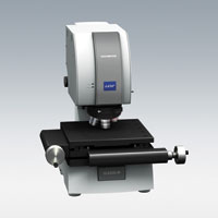 Olympus Life Science Europa GmbH has unveiled an infrared confocal laser scanning microscope for nondestructive observation of the interior of silicon wafers, integrated circuit chips and microelectromechanical systems. The OLS3000IR LEXT uses a 1310-nm laser to see through the silicon to the components, enabling inspection, measurement and analysis of system in package, 3-D mounting and chip scale package. Applications include flip chip mounting defect analysis, chip damage analysis and chip gap measurement.
http://www.olympus-ims.com
/Buyers_Guide/Olympus_Europa_SE_Co_KG/c10690
Published: September 2008
REQUEST INFO ABOUT THIS PRODUCT
* First Name:
* Last Name:
* Email Address:
* Company:
* Country:
Message:
When you click "Send Request", we will record and send your personal contact information to Olympus Europa SE & Co. KG by email so they may respond directly. You also agree that Photonics Media may contact you with information related to this inquiry, and that you have read and accept our
Privacy Policy and
Terms and Conditions of Use.
Register or login to auto-populate this form:
Login
Register
* Required