
Mask Alignment System
EV Group (EVG)Request Info
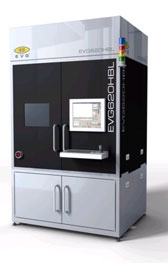
For LED manufacturing, EV Group has announced the EVG620HBL, the second-generation fully automated mask alignment system for volume manufacturing of high-brightness LEDs.
It delivers a tool platform tailored to address high-brightness LED customer-specific needs and the demand for cost-of-ownership reduction. It also optimizes tool footprint in the fab, delivering 55% higher wafer output for every square meter of cleanroom space compared to competitive offerings, according to the company.
 New features include an enhanced microscope that supports automated mask pattern search, reducing mask setup and change time; an updated robotic handling layout with wafer-mapping capability, which supports wafer traceability; improved alignment capability (line alignment), which leverages the grids that mark single LEDs for orientation instead of requiring alignment marks that take up valuable space on the wafer; and a reduced system footprint, which optimizes total cost of ownership for operation and increases the wafer per footprint index.
The company says that these enhancements result in a 20% reduction in cost per processed wafer compared to competitive offerings.
Built on a proprietary and field-proven mask aligner platform, the series features a high-intensity ultraviolet light source and an optional filter fan to maximize yield and deliver wafer throughput of up to 165 6-in. wafers per hour (up to 220 wafers per hour in first print mode).
Another feature is the availability of recipe-controlled microscopes whose illumination spectrum can be varied and optimized to ensure the best pattern contrast with various wafer and layer materials, including substrate materials such as sapphire, silicon carbide, aluminum nitride, metal and ceramic. The system processes 2- to 6-in. wafers.
For more information, visit: www.evgroup.com
https://www.evgroup.com
/Buyers_Guide/EV_Group_EVG/c4622
Published: February 2012
REQUEST INFO ABOUT THIS PRODUCT
* First Name:
* Last Name:
* Email Address:
* Company:
* Country:
Message:
When you click "Send Request", we will record and send your personal contact information to EV Group (EVG) by email so they may respond directly. You also agree that Photonics Media may contact you with information related to this inquiry, and that you have read and accept our
Privacy Policy and
Terms and Conditions of Use.
Register or login to auto-populate this form:
Login
Register
* Required