
Nanoimprint and Wafer-level Optics System
EV Group (EVG)Request Info
ST. FLORIAN, Austria, Feb. 7, 2022 — 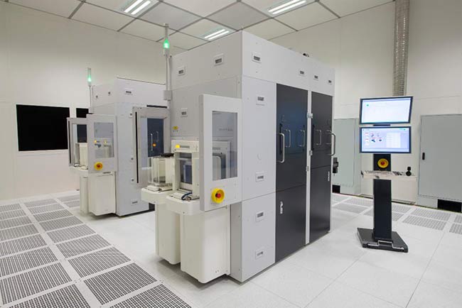 The EVG®7300 automated SmartNIL® nanoimprint and wafer-level optics system from the EV Group combines multiple UV-based process capabilities such as nanoimprint lithography, lens molding, and lens stacking in a single platform.
The multifunctional system is designed to serve advanced R&D and production needs for a wide range of emerging applications involving micro- and nanopatterning as well as functional layer stacking. These include wafer-level optics, optical sensors and projectors, automotive lighting, waveguides for augmented reality headsets, biomedical devices, meta-lenses and meta-surfaces, and optoelectronics. Supporting wafer sizes up to 300 mm and featuring high-precision alignment, advanced process control, and high throughput, the EVG7300 meets the high-volume manufacturing needs for a variety of freeform and high-precision nano- and micro-optical components and devices.
https://www.evgroup.com
/Buyers_Guide/EV_Group_EVG/c4622
Published: February 2022
REQUEST INFO ABOUT THIS PRODUCT
* First Name:
* Last Name:
* Email Address:
* Company:
* Country:
Message:
When you click "Send Request", we will record and send your personal contact information to EV Group (EVG) by email so they may respond directly. You also agree that Photonics Media may contact you with information related to this inquiry, and that you have read and accept our
Privacy Policy and
Terms and Conditions of Use.
Register or login to auto-populate this form:
Login
Register
* Required