
Piezo Scanning Stage
piezosystem jena GmbHRequest Info
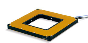
Piezosystem jena GmbH is offering the PXY AP low-profile flat and ultrafast piezo scanning stage. With its large clearance aperture, it enables the installation of diverse sample holders and other fixtures.
 For accurate scanning applications, two dedicated axis configurations are normally used: a fast axis with a long motion range, and a second axis performing small and precise steps on a line feed. The company has developed the VTR select feature, which makes it possible to combine various travel motion for different axes. Variable travel range selections from 24 to 700 µm for each axis allow adjustment of the nanopositioning system to a wide range of applications. The dynamic performances can be combined according to the specific requirements.
The integration of the bidirectional nanoX design with active resetting forces delivers high precision. Even under full load, preselected positions can be reached in milliseconds with nanometer accuracy, and the risk of overshooting is actively minimized. In combination with the integrated and proprietary high-resolution capacitive direct metrology, the stage provides accurate position stability, linearity and reproducibility in controlled motion.
Together with the MIPOS lens positioning system, the PXY AP serves as a sample table for precise imaging in 3-D microscopy.
Applications include biotechnology, nanopositioning and scanning, wafer handling, mask alignment, microscopy and materials research.
https://www.piezosystem.com
/Buyers_Guide/piezosystem_jena_GmbH/c11842
Published: April 2011
REQUEST INFO ABOUT THIS PRODUCT
* First Name:
* Last Name:
* Email Address:
* Company:
* Country:
Message:
When you click "Send Request", we will record and send your personal contact information to piezosystem jena GmbH by email so they may respond directly. You also agree that Photonics Media may contact you with information related to this inquiry, and that you have read and accept our
Privacy Policy and
Terms and Conditions of Use.
Register or login to auto-populate this form:
Login
Register
* Required