Solderable and Face Metallization Optical Coatings
Deposition Sciences Inc. (DSI)Request Info
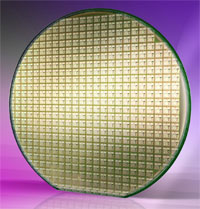
Thin film solderable coatings and face metallization coatings from Deposition Sciences Inc. are available on a wide variety of substrates with wafer-scale patterning.
 The coatings are enabled by DSI’s proprietary MicroDyn sputtering deposition technology and can be applied on virtually all optical materials. They can be combined with antireflective, bandpass or precision custom coatings from UV to LWIR wavelengths.
Typically used for hermetic sealing of sensitive packages, the coatings can also be applied to infrared detectors, cameras, focal plane arrays and other sealed sensors.
https://www.depsci.com
/Buyers_Guide/Deposition_Sciences_Inc_DSI/c3580
Published: May 2014
REQUEST INFO ABOUT THIS PRODUCT
* First Name:
* Last Name:
* Email Address:
* Company:
* Country:
Message:
When you click "Send Request", we will record and send your personal contact information to Deposition Sciences Inc. (DSI) by email so they may respond directly. You also agree that Photonics Media may contact you with information related to this inquiry, and that you have read and accept our
Privacy Policy and
Terms and Conditions of Use.
Register or login to auto-populate this form:
Login
Register
* Required