
True Surface Microscopy
WITec GmbHRequest Info
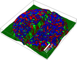
ULM, Germany, Dec. 15, 2010 — WITec GmbH has launched the True Surface Microscopy option for topographic confocal Raman imaging applications. The core element of the imaging mode is an integrated sensor for optical profilometry. Large-area topographic coordinates from the profilometer measurement can be precisely correlated with the large-area confocal Raman imaging data. This allows confocal Raman imaging along heavily inclined or very rough samples with the true surface held in constant focus while maintaining high confocality.
 With the new imaging mode, samples that had previously required extensive preparation to obtain a certain surface flatness can now be easily and automatically characterized as they are. Complete system control and extensive data evaluation are integrated within the WITec Control and WITec Project software environment, guaranteeing ease of use.
The profilometry capabilities of the modular True Surface Imaging mode enable scan ranges of up to 100 × 100 mm with a spatial resolution on the order of 100 nm vertically and 10 µm laterally. Measuring distances of 10 mm and more provide flexibility for variable sample size requirements.
In combination with atomic force microscopy (AFM), the profilometer can be used as a pre-inspection tool to determine topographic features of interest for high-resolution AFM investigations on large samples. The overall performance and high-accuracy imaging capabilities benefit many applications, including characterization of micromechanical, medical and semiconductor devices; mapping of functionalized surfaces; and imaging of biomedical and pharmaceutical materials’ surface properties.
https://raman.oxinst.com
/Buyers_Guide/WITec_GmbH/c16123
Published: December 2010
REQUEST INFO ABOUT THIS PRODUCT
* First Name:
* Last Name:
* Email Address:
* Company:
* Country:
Message:
When you click "Send Request", we will record and send your personal contact information to WITec GmbH by email so they may respond directly. You also agree that Photonics Media may contact you with information related to this inquiry, and that you have read and accept our
Privacy Policy and
Terms and Conditions of Use.
Register or login to auto-populate this form:
Login
Register
* Required