WAFER INSPECTION
Rudolph Technologies Inc.Request Info
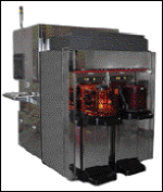 An automated inspection system for 200- and 300-mm wafers has been released by Rudolph Technologies Inc. The WaferView provides macrodefect inspection of wafer surfaces at throughputs of >100 wafers per hour. The company says the system's proprietary full-color image processing detects 95% of photolithography defects and correctly classifies them 85% of the time. The WaferView has a library of classified defects and can be programmed with new defect classes, enabling users to customize defect detection.
http://www.rudolphtech.com
/Buyers_Guide/Rudolph_Technologies_Inc/c12952
Published: March 2003
REQUEST INFO ABOUT THIS PRODUCT
* First Name:
* Last Name:
* Email Address:
* Company:
* Country:
Message:
When you click "Send Request", we will record and send your personal contact information to Rudolph Technologies Inc. by email so they may respond directly. You also agree that Photonics Media may contact you with information related to this inquiry, and that you have read and accept our
Privacy Policy and
Terms and Conditions of Use.
Register or login to auto-populate this form:
Login
Register
* Required