WAFER INSPECTION
Applied MaterialsRequest Info
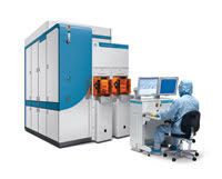 Applied Materials Inc. has unveiled its Applied UVision 3, a deep-UV bright-field wafer inspection system with the critical defect detection sensitivity required for 45-nm front-end-of-line and immersion lithography applications. The system triples the number of laser beams scanning the wafer to provide fast throughput. Two new imaging modes extend sensitivity to 20 nm, and a flexible automatic defect classification engine enables quick access to defects of interest. Imaging modes in the illumination and collection paths address the contrast versatility required for immersion lithography, and the dual-screen configuration with high-resolution review minimizes scanning electron microscopy review time. The proprietary ActiveScan technique compensates for process and color variations within and across wafers.
http://www.appliedmaterials.com
/Buyers_Guide/Applied_Materials/c989
Published: February 2008
REQUEST INFO ABOUT THIS PRODUCT
* First Name:
* Last Name:
* Email Address:
* Company:
* Country:
Message:
When you click "Send Request", we will record and send your personal contact information to Applied Materials by email so they may respond directly. You also agree that Photonics Media may contact you with information related to this inquiry, and that you have read and accept our
Privacy Policy and
Terms and Conditions of Use.
Register or login to auto-populate this form:
Login
Register
* Required