Warpage Metrology Tool
ERS electronic GmbHRequest Info
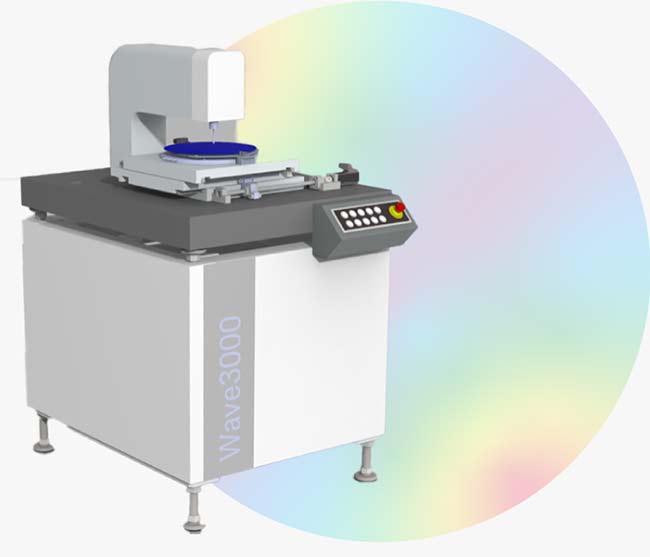 The Wave3000 warpage metrology tool from ERS electronic GmbH is designed for advanced packaging wafers and the semiconductor manufacturing industry.
The device uses advanced optical scanning methodology to accurately measure and analyze wafer deformities in specific handling positions. It can measure and analyze warped wafers from 200 to 300 mm with high precision in <1 min. The system can measure different wafer surfaces and materials, generate an interactive 3D view of the wafer, and provide insights into warpage behavior and its impact on the manufacturing process.
https://www.ers-gmbh.com
/Buyers_Guide/ERS_electronic_GmbH/c33604
Published: June 2023
REQUEST INFO ABOUT THIS PRODUCT
* First Name:
* Last Name:
* Email Address:
* Company:
* Country:
Message:
When you click "Send Request", we will record and send your personal contact information to ERS electronic GmbH by email so they may respond directly. You also agree that Photonics Media may contact you with information related to this inquiry, and that you have read and accept our
Privacy Policy and
Terms and Conditions of Use.
Register or login to auto-populate this form:
Login
Register
* Required