About This Webinar
This year is an odd and challenging one for many fields. For silicon photonics specifically, macroeconomic headwinds and concerns about war push against the tide of opportunity driven by the rapid adoption of silicon photonics technology in applications outside the gestational home of the data center. There are many examples of silicon photonics as an enabling technology including LIDAR for autonomous vehicles, new classes of weaponry, wearable technologies for health, VR headsets for entertainment, as well as new professional applications, quantum computing, and sensing.
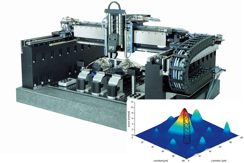
Though applications are growing, it can be disquieting to add the numbers up. As silicon photonics progresses into the mainstream, production volumes will need to ramp up by three orders of magnitude in the next few years. Professionals must consider how to build and test the novel devices and assemblies that will make this possible. It is also essential to remove costs from the manufacturing process steps that dominate overall device economics. Scott Jordan of PI considers some fundamental requirements that have emerged, such as large-area requirements for localizing, characterizing, optimizing, and tracking optical component positions for test and packaging. Groundbreaking new technology addresses these requirements, allowing fast processing of trays, carriers, circuit boards, and other large substrates. With throughputs up to one hundred times faster than previous technologies, this architecture is emerging as an enabler while the industry confronts the massive opportunities and challenges of 2023 and beyond.
Who Should Attend:
Systems engineers and optomechanical designers who utilize silicon photonics in their work. Anyone who employs precision motion systems for automated alignment, test, measurement, precision assembly, and optimization tasks. Engineers and researchers working with photonics, fiber optics, cameras, sensors, lasers, LEDs, MicroLEDs, and nanophotonics used in applications for aerospace, defense, machine vision, and semiconductors.
About the presenter:
 Scott Jordan is head of photonics for PI (Physik Instrumente) LP and is a PI fellow. A physicist with an MBA in finance/new ventures, Jordan has made multiple contributions to the fields of photonics alignment automation, precision motion control, and optimization technologies.
About PI (Physik Instrumente):
PI (Physik Instrumente) LP designs and manufactures high performance motion systems at locations in the U.S., Europe, and Asia. Industries and fields of application include silicon photonics wafer test, fiber alignment, laser processing, life sciences and microscopy, astronomy and aerospace, medical engineering, and big science projects. With 50 years of experience developing standard and custom motion and piezo products, and with more than 1500 employees in 15 countries, PI can quickly move customers’ positioning and automation projects forward.