About This Webinar
Integrated circuit (IC) manufacturing already requires the use of advanced technology nodes down to 5 nm, and has roadmap plans requiring 2 nm for production within the next couple of years. The complexity associated with these advanced nodes, together with the use of new materials, poses challenges for specific chemical mechanical polishing (CMP) processes that aim to achieve nanometer-level flatness along each die on a wafer. Flatness has always been an important goal for CMP, but for advanced IC, it is an even more stringent parameter, as it enables the stacking of an increased number of layers for NAND memory, separation of logic, and active pixel areas in CMOS imaging sensors, as well as delivering further heterogeneous integration via die-to-wafer bonding for high-performance computer (HPC) usage.
This webinar discusses how optical profiling, based on white-light interferometry (WLI), provides unique nanometer accuracy in die flatness assessment while retaining micron lateral resolution. Measurement examples on CMP testing wafers offers solid evidence that flatness of full die can be achieved with nanometer reproducibility in a timely manner to match the stringent CMP qualification needs. Thanks to advanced stitching algorithms, data over the full die map captures both T check boxes and topography effects from variation of pattern density.
This presentation also covers how hot spots, unwanted erosion, or dishing down to submicron details all can be automatically identified along the die map, as well as changes of CMP performance across the complete 300-mm wafer. Finally, the presenter will discuss using this same WLI metrology platform for other challenging applications in advanced packaging, such as characterizing TSV (through silicon via) and overlay between layers.
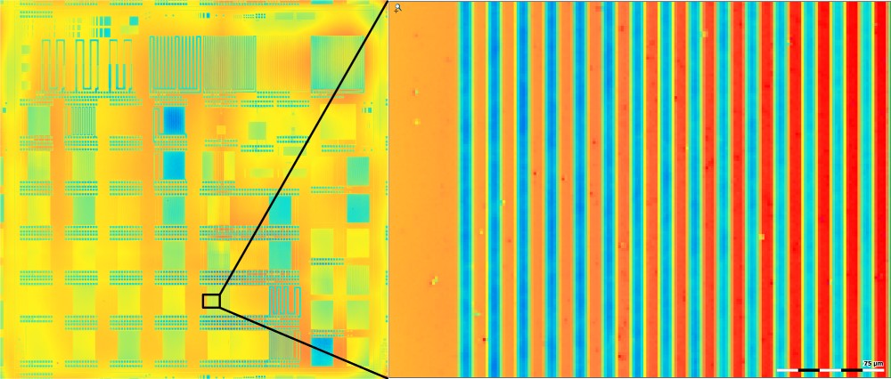
On left, top-view topography of full die (21 × 21 mm²) from test wafer after CMP process. On right, digital zoom illustrating lateral resolution with some defects circled in white. Courtesy of Bruker.
Who should attend:
Engineers, researchers, QA and QC professionals, optical designers, and executives and managers concerned with metrology for CMP optimization as it applies to a range of industries, including semiconductors and microelectronics, additive manufacturing, automotive, and aerospace.
About the presenter:
 Samuel Lesko, Ph.D., has over 18 years of optical profiler applications experience, particularly in using white-light interferometry in a wide variety of fields, from MEMS and semiconductor to automotive and aerospace. Lesko obtained his Ph.D. in physics and material science engineering degree at the University of Burgundy in France; email: [email protected].
About Bruker:
Bruker is the worldwide leader in 3D surface measurement and inspection, offering fast, noncontact analyses for samples ranging in size from microscopic MEMS to entire engine blocks. Bruker microscopes are the culmination of 10 generations of proprietary Wyko® Technology advances that provide the high sensitivity and stability necessary for precision 3D surface measurements in applications and environments that are challenging for other metrology systems. Bruker’s high-performance scientific instruments and high-value analytical and diagnostic solutions enable scientists worldwide to explore life and materials at molecular, cellular, and microscopic levels.