About This Webinar
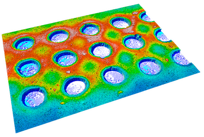
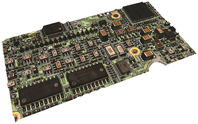
This webinar will discuss specific analysis for QC in PCB
applications. It will also cover critical dimensional measurement, roughness, and
defect identification. Presenters Adam Platteis and Alberto Aguerri will show solutions pertaining to ISO 4287, ISO 25178, and how Sensofar's proprietary software quickly identifies profiles, roughness parameters, and defects for surface texture, height, and traces. The focus will be on imaging wafers, pads, step heights, bonds, and probe cards.
Sensofar solutions can be used in the R&D lab and for in-line QA/QC high-throughput environments for automatic Pass/Fail reporting. Sensofar offers stand-alone and customizable solutions that integrate confocal, interferometry, and focus variation technologies into a single sensor-head for the semiconductor and microelectronic industries.
About the presenters:

Adam Platteis, a graduate of York College, joined Sensofar in 2018 as the company’s U.S. sales manager. Before joining
Sensofar Metrology, Platteis spent 10 years with Carl Zeiss Microscopy, providing
solutions to the semiconductor, microelectronics, and other industrial markets.

Alberto Aguerri is the vice president of sales for Sensofar Metrology. He has worked for Sensofar for more than 10 years in various company positions. Before joining Sensofar, he worked for several years as an application engineer in fields related to optical metrology. Aguerri holds a MSc in photonics from Polytechnic University of Catalonia (UPC).
Who should attend:
This webinar is for R&D managers, lab technicians, QA and QC professionals, inspection managers, engineers, process integrators, wafer technicians, and anyone involved in failure analysis and/or material analysis. Professionals working in the semiconductor and microelectronics fields will benefit from this webinar, as well as those involved in precision optics, data storage, display technologies, and film and material technologies.
About Sensofar:
Sensofar is a leading-edge technology company that has the highest quality standards within the field of surface metrology.
Sensofar Metrology provides high-accuracy optical profilers based on confocal, interferometry, and focus variation techniques, from standard setups for R&D and quality inspection laboratories to complete noncontact metrology solutions for in-line production processes. The Sensofar headquarters are located in Barcelona and the Group is represented in over 30 countries, with sales offices in Asia, United States, and Germany.