About This Webinar
Contemporary manufacturing processes go beyond simple stamping, molding, or CNC machining steps, and adopt more advanced technologies, such as additive manufacturing and 3D printing. While the gains in design flexibility and part complexity are obvious, there are many process parameters behind the scenes that, together with the necessary finishing steps, are critical to meeting roughness, aesthetic, or functional requirements.
This webinar illustrates how advanced optical profiling accurately assesses complex surface textures through areal roughness parameters (from the ISO25178 norm), as well as how the same profiler can be used to optimize subsequent finishing steps, from bed fusion of metallic powder to polymer-printed surfaces. Attendees will learn how efficient areal roughness parameters within these new manufacturing processes supersede Ra, and which parameters to select that will directly tie to the effectiveness of processes, the shininess/appearance of parts, and the quality of the 3D printing. A Q&A session will close the event.
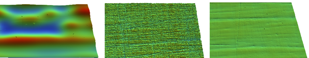
Example of optical profiling for a variety of surface textures. Courtesy of Bruker.
Who should attend:
Quality control, metrology, material development, additive and 3D-printing manufacturing engineers, finishing process designers (e.g., blasting, tumbling, polishing, laser texturing), and others interested in controlling the quality of the finishing steps for additive-manufactured or 3D-printed parts. This webinar is applicable to a variety of industrial markets, including aerospace, automotive, energy, medical, and semiconductors.
About the presenter:
 Samuel Lesko, Ph.D., is director of applications development for stylus and optical profilers and tribology at Bruker. He has over 20 years of optical and stylus profiler applications experience, particularly in using white-light interferometry in a wide variety of fields, from MEMS and semiconductor to automotive and aerospace. He is a member of SME and part of ISO/TC 213/WG committee (areal roughness). He obtained his physics Ph.D. and material science engineering degree at the University of Burgundy in France; email: [email protected].
About Bruker:
Bruker is the worldwide leader in 3D surface measurement and inspection, offering fast, noncontact analyses for samples ranging in size from microscopic MEMS to entire engine blocks. Bruker’s optical profilometers are the culmination of 10 generations of proprietary Wyko® Technology advances that provide the high sensitivity and stability necessary for precision 3D surface measurements in applications and environments that are challenging for other metrology systems.