Echelle gratings compete with arrayed waveguide gratings for complex, high-channel-count optical integrated circuit applications.
Dr. Sylvain Charbonneau and Dr. Matthew Pearson
The demand for increased communications bandwidth in North America is rapidly being
replaced by demands for technology that will allow service providers to use existing
optical capacity more efficiently and profitably. Consequently, a growing number
of component manufacturers are focusing resources on developing cost-effective solutions
for multiplexing and demultiplexing wavelengths.
Many of these companies are turning to planar
waveguide devices to deliver complex optical integrated circuits that offer increased
scalability and superior performance at a lower cost. As optical networks evolve
to higher channel counts at lower cost, the currently popular arrayed waveguide
gratings may not be able to satisfy future system demands in terms of performance,
cost and manufacturability.
However, the echelle grating has quietly
matured to a stage where it can outperform arrayed waveguide gratings in nearly
all respects, at a fraction of the cost and while using a fraction of the power.
Although the operating principles of
echelle and arrayed waveguide gratings are similar, their layouts are very different.
In an arrayed waveguide grating (Figure
1, left), light of various wavelengths enters the input waveguide (1) and travels
to a slab waveguide region (2) that divides the power among the more than 100 waveguides
in the grating array (3). Each waveguide has a precise length difference relative
to its neighbors so that its light emerges from the end of the array section with
a different phase delay. A second slab waveguide region (4) focuses the light from
all the waveguides onto the output waveguide array (5). Because each wavelength
has a precise differential phase tilt, each one focuses into a different output
waveguide. Optical fibers then carry the wavelengths individually off the chip.
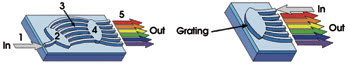
Figure 1. In an arrayed waveguide grating
(left), each channel or wavelength of light enters a waveguide that delays its phase.
A second waveguide focuses the result into the output waveguide array. In an echelle
grating (right), reflective facets diffract and focus each channel into the output
waveguide array.
Arrayed waveguide grating devices have
shallow, etched ridge waveguides, which are relatively simple to fabricate on low-channel-count
devices. (Additional processing steps are required to achieve polarization insensitivity.)
In an echelle grating demultiplexer
(Figure 1, right), light couples into a single-mode input ridge waveguide and into
a slab waveguide region similar to that found in an arrayed waveguide grating. The
light then diverges in the two-dimensional waveguide until it arrives at the grating
on the opposite end of the chip.
The echelle grating is vertically etched
into the planar waveguide to a depth much greater than the waveguide mode width,
and the grating facets are coated with a reflective material to create a series
of stepped mirrors. The curved grating both diffracts and focuses the light onto
one of a series of deeply etched output waveguides situated on the same side of
the chip as the input waveguide. The output waveguides move the individual wavelengths
off the chip and couple the light to optical fibers.
Silica-on-silicon
Several years ago arrayed waveguide gratings became
the primary choice for high-channel-count dense wavelength division multiplexing
applications. At that time, echelle grating manufacturing technology could not effectively
etch the gratings because of the depth of the etch and the requirements for verticality
and smoothness. Recent advances in semiconductor manufacturing technology and the
use of silica-on-silicon are enabling echelle grating manufacturers to offer products
with increased scalability and functionality.
Regardless of the planar device, silica-on-silicon
is the most common material choice for optical waveguides because silica’s
refractive index profile is very similar to that of optical fiber, which minimizes
coupling losses. Planar device manufacturing uses two deposition techniques: chemical
vapor deposition and flame hydrolysis deposition. Chemical vapor deposition, a modification
of standard semiconductor processing, is compatible with cleanroom processes and
with high-volume wafer production.
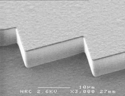
Figure 2. Manufacturing
challenges have hampered echelle gratings in the marketplace, but new reactive ion
etch technology can create deep facets with excellent verticality and smoothness.
For echelle grating devices, verticality
and smoothness of the deeply etched grating facets are critical. To fabricate waveguides
and gratings in silica-based materials, manufacturers use reactive ion etching.
This technique can achieve grating wall verticality better than 89.8° with
a root mean square roughness better than 30 nm over 30 μm on a production tool
(Figure 2). However, reliability and reproducibility continue to challenge some
companies that are developing and commercializing echelle grating technology.
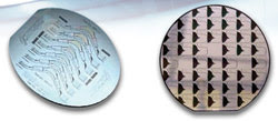
Figure 3. A 6-in. wafer can hold more than five times as many 40-channel echelle grating
demultiplexers (right) as arrayed waveguide grating demultiplexers (left).
Still, those that can manufacture these
devices can offer customers some performance advantages over arrayed waveguide devices:
• Size. One 6-in. wafer
can hold seven 40-channel arrayed waveguide grating demultiplexers (Figure 3, left)
or 38 echelle grating demultiplexers (Figure 3, right). The echelle grating device
transfers directly into a small package (Figure 4). An echelle grating mux/demux
is about one-quarter the size of a comparable arrayed waveguide grating device.
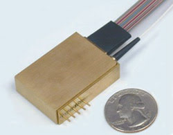
Figure 4. A 40-channel echelle grating demultiplexer packaged with
thermoelectric cooler and thermistor is about one-quarter the size of a comparable
arrayed waveguide grating device.
The smaller form factor allows manufacturers
to integrate more functionality on a chip or to integrate the device with an InGaAs
detector array to produce very small optical channel monitors suitable for embedding
directly in network elements. This type of functionality and integration has long
been envisioned as the future of optical components; however, arrayed waveguide
gratings’ size and yields have hampered its execution.
• Crosstalk. Device size
hampers arrayed waveguide grating crosstalk performance because phase errors accumulate
along the length of the waveguides. Echelle gratings eliminate this problem by replacing
the arrayed waveguides with an etched grating. Phase errors in echelle gratings
result solely from errors in the positions of the grating facets and depend only
on facet fabrication accuracy.
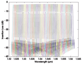
Figure 5. Size gives echelle grating demultiplexers some performance
advantages compared with arrayed waveguide grating devices. The graph shows insertion
loss characteristics of a 49-channel echelle grating demultiplexer: die size, 18
x 20 mm; adjacent channel crosstalk, 35 dB; background channel crosstalk, 37 dB.
These errors are of two types: rounding
errors, resulting from the finite step size of the mask, and stitching errors,
which occur when small write fields are stitched together to form a large element.
Because arrayed waveguide gratings
are so large, it is unlikely that they can be written in a single field. These fundamental
design issues result in better performance in echelle gratings. However, all manufacturing
processes must still be highly uniform and tightly controlled to achieve high isolation.
Process control remains the key to high performance.
• Insertion loss. Insertion
loss is the sum of the coupling and on-chip losses. Coupling losses are almost identical
for arrayed waveguide and echelle gratings. Unlike discrete demultiplexers, planar
waveguide demultiplexers’ insertion losses are very uniform (less than 1 dB
across the whole wavelength range) and do not scale with channel count.
On-chip losses are the result of fundamental
material and scattering losses due to structures on the chip. Because the optical
path length in an echelle grating is typically smaller than that of an arrayed waveguide
grating, its material and scattering losses are also smaller.
• Scalability. Scalability
to high channel counts has led many systems manufacturers to shift from thin-film
filters to planar waveguide components. Arrayed waveguide gratings have been the
choice for this type of integration. However, component size restrictions and accumulated
phase errors make it difficult to scale these devices to 80 channels or more. Typically,
one 6-in. wafer can hold about four 80-channel arrayed waveguide gratings, but wafer
nonuniformities and processing defects commonly reduce the ultimate yield to two
devices — or fewer.
Echelle grating demultiplexers, in
contrast, can easily scale to 80 channels, with more than 30 fitting on a 6-in.
wafer. The small size of the devices also makes them less affected by wafer nonuniformities.
Echelle grating demultiplexers are available in 160-channel configurations and have
been demonstrated at 256 channels. Currently, the only limit for these devices is
the large fan-out for fiber attach.
• Power consumption. Both
devices consume power to regulate temperatures and maintain thermal stability for
optimum channel tuning. Arrayed waveguide gratings are packaged with thermoelectric
coolers or heaters and thermistors to monitor temperature. Echelle gratings need
thermal stability only across the relatively small free propagation region. As a
result, their power requirements are typically one-half to one-fifth of those of
comparable arrayed waveguide gratings. Several companies are developing athermal
gratings of each type. At present, manufacturing costs restrict their widespread
deployment.
Integrated circuits
Perhaps the most important benefit of echelle
grating technology is that it offers the ideal platform on which to pattern further
functionality. The size of arrayed waveguide grating demultiplexers makes this difficult,
especially at high channel counts. Yields are already so low that adding further
functionality would significantly increase manufacturing costs.
On the other hand, manufacturers are
coupling echelle gratings with attenuation and switching functions to develop a
new form of planar lightwave circuit: the readily customizable photonic application-specific
integrated circuit.
In its simplest form, such as integrated
circuit would comprise a custom demultiplexer and hybrid detector arrays to create
devices such as embeddable optical channel monitors. Variable optical attenuation
and switching technology will bring true customization to this platform, enabling
its use in fully configurable optical add/drop modules and customer-specific designs
for planar lightwave circuits.
Meet the authors
Sylvain Charbonneau is chief technology officer
at Optenia Inc. in Ottawa. He has a PhD in semiconductor physics from Simon Fraser
University.
Matthew Pearson is a product manager at Optenia.