David Collier and Wayne Pantley
Producing long-lifetime optics for cutting-edge microlithography at 157 nm has presented a
major challenge to optics manufacturers. Keeping contamination and surface damage
under control is key.
When microlithography at 157 nm was first being investigated several years ago, optics
that could survive 10 million laser pulses were the benchmark of performance. Today,
pulse-count lifetimes of 40 billion pulses represent the state of the art. To achieve
this, virtually every aspect of the traditional fabrication of deep-UV optics, including
coating, testing and packaging processes that are used for longer-wavelength components,
has had to be reviewed and refined.
Progress in each of these areas has resulted in
major improvements in optics lifetime and performance. The technology developed
for 157-nm optics has also been used to produce better performance at other deep-UV
wavelengths, such as 193, 248 and 266 nm. But producing these optics is no mean
task; many practical aspects must be taken into consideration.
Component cleaning
The most significant issues confronted when shaping
and polishing 157-nm optics are related to contamination, tolerances and materials.
Contamination is of particular concern because most of the substances traditionally
used for processing optics, such as polishing compounds and cleaning solvents, absorb
strongly at that wavelength. Also, many common environmental contaminants (human
perspiration, machine oil, airborne particulates from other polishing operations)
absorb at 157 nm, even when present in trace amounts.
Because avoiding contamination is imperative,
surfaces must be cleaned frequently, and the cleaning process must be carefully
monitored so that it does not leave its own residual contamination. The types of
solvents used, their purity and handling must all be controlled. Acetone is probably
the most commonly used, but combining high-purity acetone with spectroscopic-grade
methanol, or using methanol alone, is usually a better solution for cleaning deep-UV
optics. Other nonchemical surface-cleaning technologies originally developed for
the semiconductor industry can be employed as well.
Grinding and polishing
Tolerances are a problem at 157 nm, partly because
the wavelength is so short. A λ/10 flatness specification at 157 nm, typical
for microlithography components, translates into a surface that is more than four
times as flat as the same specification at 633 nm. The difficulty in achieving this
flatness is compounded when working with crystalline materials, such as CaF2, which
are essentially the only option for transmissive optics at 157 nm.
Excellent surface quality (scratch-dig)
and minimal defects are of paramount importance in achieving high-throughput, deep-UV
optics. A typical scratch-dig specification for 157-nm optics is 20-10 or better.
Good surface quality also delivers higher damage threshold, even at longer wavelengths.
However, CaF2 is anisotropic, hygroscopic
and very prone to chipping and fracturing. During polishing, it is not unusual for
small particles to break loose from the part edge and be dragged over the component
surface, causing scratches. As a result, achieving a given surface quality specification
usually requires 50 to 100 percent longer polishing times for CaF2 than for fused
silica. But a longer polishing time typically makes it more difficult to achieve
a high-flatness (or surface figure for spherical or cylindrical parts) specification.
Because of this trade-off, it is substantially
more difficult to consistently fabricate tightly toleranced CaF2 components on a
production basis as compared with harder, noncrystalline materials. In addition,
the process requires a more careful balance between the various process parameters
(polishing time, spindle speed, spindle pressure, etc.) to simultaneously meet both
shape and surface quality specifications.
These working characteristics of softer,
crystalline materials necessitate modifications to the standard polishing approach.
For example, the grinding process for CaF2 requires more steps and must be performed
to a finer level than is typical with harder materials such as glass or fused silica.
The traditional grinding and polishing tools require some modification. At Alpine
Research Optics, we use a softer pitch lap for CaF2, and cut it differently to enable
heavier particles to be removed faster, thus avoiding scratches. It is also important
to avoid thermal shock during processing; for example, not putting cold solvents
on parts that have been warmed by the polishing process.
The need to scrupulously avoid any
contamination also requires a change in the type of polishing compounds used. Ceria
(CeO2), which is a commonly used abrasive for optics polishing, absorbs strongly
at short wavelengths. It is virtually impossible to eliminate all of the residual
polishing compound from an optical surface because some of it becomes embedded under
the surface during processing.
Therefore, alternative abrasives that
have lower absorption at 157 nm must be used. We have found success with a diamond-based
abrasive mixed with deionized water. The mixture is added manually during the polishing
process and used only once, rather than recirculated in a slurry, as in conventional
optics polishing. However, even diamond-based abrasives can contain impurities that
absorb in the deep-UV. We have found it necessary to qualify our abrasives vendors
because not every supplier can consistently deliver products with the required purity
level.
It is also important to avoid subsurface
damage in the production of low-absorption, high-damage-threshold, deep-UV optics.
Subsurface damage, a phenomenon first identified by researchers at Lawrence Livermore
National Laboratory in Livermore, Calif., consists of fractures and scratches that
occur during the grinding and polishing process and that become partially or totally
covered by the polishing redeposition layer (Figure 1). This is a thin layer of
material that flows while the material is being worked and that covers the surface.
It is through this mechanism that residual polishing compound may become incorporated
into the surface layer itself or deposited in microfractures and surface defects.
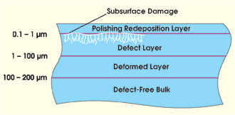
Figure 1. Subsurface
damage causes fractures and scratches that occur during the grinding and polishing
process to become partially or totally covered by the polishing redeposition layer.
Using a sequence of successively finer
grinding and polishing steps minimizes subsurface scratching and ensures that each
step removes sufficient material to eliminate any damage caused by the previous
step. When working with soft materials, it also may be necessary to use lighter-weight
grinding tools, as opposed to traditional cast-iron tools, because heavier implements
have a greater tendency to create small fractures in the material.
The need to avoid contamination also
means that any deep-UV fabrication equipment should be devoted solely to that purpose.
Furthermore, the production area should be environmentally isolated to prevent problems
from airborne particulates produced by other polishing operations.
Thin-film coating
There are many potential contamination sources
in the optical thin-film coating process. As in all traditional coating operations,
parts must be cleaned first. Once the deep-UV optics are in the coating chamber,
additional surface cleaning takes place. Because the chamber itself can be a source
of contaminants, it must be made hydrocarbon-free by using oil-free, dry mechanical
pumps and cryopumps.
The coating process involves heating
substrates to a high temperature, which also heats the interior of the coating chamber
and can cause the residue of any materials from previous coatings to evaporate and
redeposit on the optics. Obviously, regular cleaning is necessary, but it is best
to avoid applying other coatings that would leave difficult-to-remove residues.
It may not be practical for a manufacturer to devote a coating chamber solely to
deep-UV coatings. However, using the same chamber for production of both deep-UV
and infrared coatings must be avoided.
Another potential source of impurities
is the coating material. Rather than assaying the chemical composition of all incoming
coating materials, the most practical procedure is to work with vendors to achieve
a consistent supply of high-purity materials.
The tiny number of coating materials
available for use at 157 nm places limitations on both the design and manufacture
of thin films. Only fluoride materials are transmissive at this wavelength, and
these are limited to delivering coating layers over a relatively narrow refractive
index range. For a typical λ/4 stack, high-reflection coating, the coating bandwidth
is directly related to the index ratio between the high- and low-index layers. Thus,
a smaller index split results in a narrower-bandwidth coating (Figure 2).
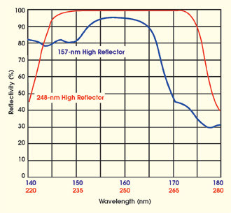
Figure 2. The reflectivity of high-reflection coatings for 157 and
248 nm are plotted to nearly the same scale, in terms of percentage. The 248-nm
coating has a bandwidth of approximately ±6 percent, while the 157 nm has a
bandwidth of only about ±1 percent. This makes it more difficult to reliably
produce a coating with a narrower bandwidth.
This means that layer thickness must
be more closely controlled during deposition, because to meet specification, a narrow-bandwidth
coating must be accurately centered on its operating wavelength. However, the difficulty
in achieving this accuracy is compounded by the fact that the layers themselves
are very thin: A λ/4-thick layer at 633 nm is four times thicker than a λ/4 layer
at 157 nm. Therefore, achieving a particular percentage accuracy in the layer thickness
requires four times greater accuracy.
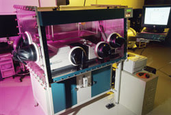
Figure 3. Because oxygen absorbs deep-UV radiation, performance
testing must be performed in a pure, dry nitrogen atmosphere. This deep-UV spectrophotometer
measures the transmission characteristics of coated parts.
The use of only fluoride materials
also affects the mechanical characteristics of the coatings. High-reflection coatings
for longer wavelengths usually alternate materials such as HfO2 and SiO2, which
produce layers under tensive and compressive stress, respectively. By alternating
layers with opposite stress characteristics, the net result is a thin film that
is in mechanical equilibrium.
In contrast, a fluoride-only material
coating will be tensive and could be prone to crazing. This limits the number of
layers that can be deposited, which again reduces coating bandwidth and peak reflectivity.
It is possible to minimize coating stress by performing deposition at the highest-possible
temperature because this produces denser, more mechanically stable layers. However,
when such a coating is cooled to room temperature, any mismatch in thermal expansion
coefficient between the coating layers and substrate can introduce stress, making
the film mechanically unstable. This trade-off, which must be optimized through
practical experience, involves combining accurate process data logging for each
coating run with actual lifetime results from end users. Participation in independent
testing, such as that performed in the Massachusetts Institute of Technology’s
Sematech program, is an important component in supplying feedback for this process.
Packaging
For deep-UV optics to maintain their performance
after delivery to a customer, the same care in avoiding contamination must extend
to their final destination. For 157-nm optics, traditional part packaging, which
utilizes lens tissue, plastic bags and foam packing material, may not be adequate.
All packaging materials should be inert and not outgas. The latter is important
because the product may be exposed to extremes in temperature and even pressure
(e.g., in an airplane hold) during shipping. Part containers made of inert materials
are available that securely hold the part by the corners or outside of the clear
aperture, eliminating the need for wrapping and packing material (Figure 4).
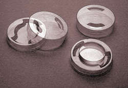
Figure 4. Modern packaging methods for deep-UV optics eliminate the
use of wrapping and packing materials that may outgas.
Further refinements in materials and
ongoing process improvements will continue to push this performance forward. The
results will benefit microlithography users as well as applications at other deep-UV
wavelengths in biomedicine, electronics packaging and industrial micromachining.
Meet the authors
David Collier is president of Alpine Research Optics in Boulder, Colo.
Wayne Pantley is the company’s sales manager.