The demands of telecom have advanced optical thin films for applications such as biotechnology.
Turan Erdogan and Victor Mizrahi, Semrock Inc.
Multilayer optical thin-film filters play a critical role in applications ranging from biomedical and analytical instrumentation to advanced laser systems. Although many of these applications still rely on outdated filter technology, there is light at the end of the tunnel, thanks to recent advances in optical thin films driven by the rigorous demands of the telecom industry.
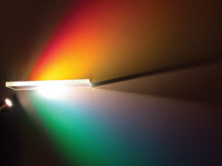
The demands of telecom have advanced optical thin films for applications such as biotechnology.
Optical thin-film filters typically consist of multiple alternating layers of high- and low-refractive-index material deposited on a glass substrate. They work based on the wavelength-dependent interference of light reflected or transmitted at the many interfaces between the layers.
This filter technology took a revolutionary step forward as a result of developments driven by the challenging requirements of dense wavelength division multiplexed (DWDM) optical communications systems. Because of low loss, excellent spectral performance and capability for passive temperature compensation, thin-film filters rapidly became a key component technology that enabled the deployment of higher-performance, lower-cost fiber optic systems.
The significance of this advance is perhaps best summarized by Angus Macleod of Thin Film Center Inc. in Tucson, Ariz.: “The telecom field has been characterized by requirements for substantial improvements in virtually every aspect of thin-film optical coating design, manufacture and performance, and all of this has had to be accomplished in the shortest time imaginable. A decade ago we would have said that today’s achievements would be impossible.”1
Perhaps the first key development was the demonstration of extremely narrow bandpass filters at wavelengths near 1550 nm for selecting individual channels in a DWDM system that are spaced first by 1.6 nm (200 GHz), and then by 0.8 nm (100 GHz). These filters, first publicized by Optical Coating Associates and soon thereafter by others, such as Optical Coating Laboratory Inc. in Santa Rosa, Calif., were based on multiple Fabry-Perot cavity designs that comprised quarter-wavelength-thick layers of high- and low-index hard oxide materials. These also were thicker and had more layers than had previously been thought possible for thin-film filters.
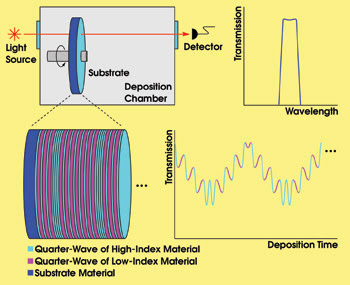
With turning-point monitoring, used primarily for making narrow bandpass filters, it is possible to produce quarter-wavelength-thick layers by terminating the deposition of the high- or low-index material when the measure of transmission vs. time reaches a maximum or minimum.
Multichannel filters
Since then, the technology has continued to advance, with companies demonstrating filters for channel spacings as small as 0.2 nm (25 GHz) and those capable of transmitting eight 100-GHz-spaced channels while reflecting all immediately adjacent channels (an 8-skip-0 filter).2,3 Because of the highly rectangular spectral shape (very small ratio of edge steepness to bandwidth) required by such filters, some need up to 17 Fabry-Perot cavities and more than 400 total layers.
Another key development was the demonstration of thin-film-based gain-flattening filters, which flatten the gain spectrum of fiber optic amplifiers by providing a precisely defined loss spectrum.4 Fewer companies developed this technology because of the challenges of designing and manufacturing these filters, many of which required layers that were all nonquarter-wavelength thick.
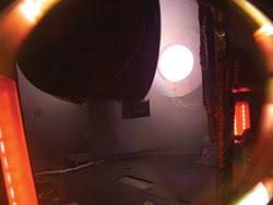
This shows the inside of a modern ion-beam sputtering deposition system, taken through one of the port windows.
Three main ingredients made this advance in thin-film filter technology possible: deposition technology, filter design and optical monitoring. The deposition technology that existed 10 years ago was incapable of making the optical filters needed for today’s high-capacity multiwavelength telecom systems. These high-performance filters are tens of microns thick and require hundreds of layers. New deposition approaches with the ability to fabricate filters over a small area but with extremely high uniformity and a stable deposition rate had to be developed.
An important technology that emerged was ion-assisted ion-beam sputtering. Besides the high degree of control afforded by this approach, it is based on hard oxide materials able to withstand the rigorous environmental durability demanded by telecom applications. The coatings had to be “nonshifting” when exposed to damp heat, and able to operate over a wide range of temperature and humidity conditions for many decades without failure.
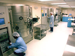
Ion-beam sputtering deposition systems developed for the production of telecom filters can produce thin-film filters for applications such as biomedical and analytical instrumentation.
The second enabler involved advances in filter design. With so many layers, the new designs pushed the envelope of commercial software, requiring new algorithms. Designers had to learn how to make extremely narrow and rectangular bandpass filters with minimal ripple, and the spectral performance had to be robust to deal with manufacturing variations and environmental fluctuations.
Gain-flattening filters, mostly based on nonquarter-wavelength-thick layers, opened up a whole new design space, and a myriad of algorithms were devised to design filters with extremely small deviations from the loss-spectrum target curves. However, although the use of nonquarter-wave-length layers simplifies the design, it complicates the fabrication.
The third key development involved highly sophisticated optical monitoring algorithms and hardware. In optical monitoring, one measures the transmission through the coating during the deposition process and uses the resulting information to decide when to stop depositing one material and start depositing the next. It was clear that, for telecom, the filter itself had to be monitored, rather than a “witness sample” somewhere else in the deposition chamber.
For bandpass filters, engineers took advantage of the elegant technique of turning-point optical monitoring, in which quarter-wavelength-thick layers are terminated at a turning point in the measured transmission-vs.-time curve (where the transmission changes from decreasing to increasing, or vice versa). With this technique, thickness errors do not accumulate rapidly. Instead, they are compensated for in subsequent layers as long as the prescription of terminating layers at the turning points is maintained. Without this self-correcting feature, random thickness errors would have to be kept much smaller than lengths comparable to the atomic spacing — an obviously impossible feat.
Subsequently, algorithms were developed for monitoring gain-flattening filters. These proved much more difficult to implement because of the nonquarter-wavelength-thick layers, which could not take advantage of the self-correcting nature of turning-point monitoring. Thus, filters made of such layers required highly sophisticated optical monitoring algorithms.
New opportunities
The technological advances that were spurred by optical communications systems are ripe for application to a wide variety of other established and emerging markets. Properly harvested, these advances in thin-film filter technology can be and are being leveraged to create high-performance optical filters for markets such as biomedical optics and analytic instrumentation systems.
A number of significant hurdles must be overcome, though, to reap the benefits of telecom thin-film filter technology across diverse applications, many of which require filters for visible or near-IR wavelengths. These filters are much larger than their telecom counterparts (typically 25 mm as compared with ~1 mm for telecom filters). The shorter wavelengths imply thinner layers and a shorter deposition time per layer, making precise optical monitoring much more challenging.
Problems with optical monitoring in the visible and near-IR are exacerbated by the lack of bright, widely tunable light sources like the tunable semiconductor lasers typically used for monitoring in the ~1550-nm telecom window. A larger filter size means the yielded output per coating run is substantially smaller for a given coating area, so significant advances must be made to extend the usable area over which accurate coating thickness can be maintained. Despite the magnitude of these hurdles, optical engineers are conquering them, making it possible to viably manufacture filters for various applications:
• Fluorescence technology. Most fluorescence instruments use thin-film filters to isolate and separate excitation and emission light. They include fluorescence microscopes for imaging biological matter, microarray readers for DNA sequencing and analysis, high-throughput screening systems used widely in drug discovery, and flow cytometry systems for counting and sorting blood cells or other biological matter. Fluorescence is also widely used in chemical process monitoring.
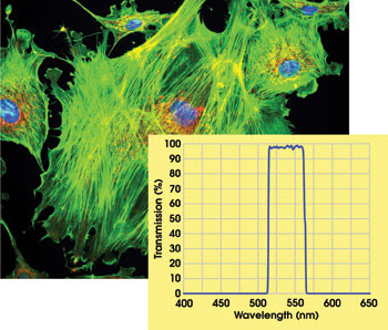
Taken with an Olympus BX41 fluorescence microscope, this multicolor exposure of bovine pulmonary artery endothelial cells uses the latest generation of fluorescence filters (see inset). Note the very high and flat passband transmission and the steep sides of the fluorescence emission filter shown. This near-ideal rectangular profile is reminiscent of the best demultiplexing filters used in modern high-data-rate optical communications systems.
Filter types include bandpass filters, long- and short-wave-pass filters, and dichroic beamsplitters. Good filters have high transmission in passbands, steep and accurately located edges for separating the fluorescence signal from undesired light, and high blocking of all other background light. Significant performance advantages, such as steeper edges, are possible using coatings that are tens of microns thick with well over 100 nonquarter-wavelength-thick layers.
But it is not only the spectral performance of these filters that benefits from recent advances. High-performance fluorescence filters used in microscopes must also exhibit excellent imaging quality. Because of the precision now achievable with hard coatings, complex fluorescence filters can be made by depositing the coatings on the outer surfaces of a single piece of glass.
In contrast, what were until recently state-of-the-art fluorescence filters have traditionally been produced using multiple substrates with soft coatings. These were arranged in such a way as to protect the coatings from the environment, often employing optical adhesives to combine substrates. Such a complex structure increases loss as well as distortion in the transmitted image. It is particularly difficult to eliminate beam deviation caused by the wedge angle of the overall filter structure.
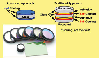
The structure of modern high-performance fluorescence filters (left) is much simpler than more traditional filters (right) and requires no adhesives in the optical path. This structure leads to lower loss, greater reliability and better imaging qualities. Inset: filters for both microscopy and instrumentation.
In fluorescence microscopy, multiple images produced with different filter sets are often overlaid, and any beam deviation causes poor image registration. Putting hard coatings on a single piece of glass virtually eliminates these problems. In this case, the transmitted wavefront distortion is determined by the single glass substrate, which can be readily manufactured to extremely high tolerances.
In many fluorescence filter applications, high reliability and durability are also important. This is particularly true for instruments used in high-throughput diagnostic or research laboratory settings. Fluorescence filters produced using hard coatings are inherently reliable, as are their pedigree telecom filters. The hard oxide coatings are as hard as the glass substrate itself. Handling is simplified because end users can employ standard solvent techniques to clean filters without fear of damaging them.
In addition, because the single-substrate design has no epoxies in the optical path, one need not worry about damage caused by excessive optical power or the effects of prolonged high temperature and humidity. Filter reliability is proved out in environmental test chambers of the type used in telecom component testing.
• Raman spectroscopy. In this technique, a laser excites a test sample, and the spectrum of the scattered light to the long-wavelength (Stokes) or short-wavelength (anti-Stokes) side is analyzed to yield information about the constituents of the sample. From the pattern of spectral lines, one may identify established “fingerprints” for various elements and/or molecules. Although some kind of dispersive instrument, such as a grating monochromator, is needed to analyze the spectrum, a static prefilter is essential to suppress the scattered laser light and to avoid overwhelming the measurement system.
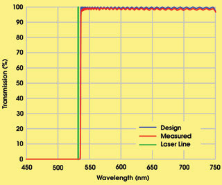
This new-generation Raman edge filter helps eliminate scattered light from a frequency-doubled Nd:YAG excitation laser at 532 nm (laser line shown in green) while passing the information-containing Raman signal band. It features an extremely steep edge, high and wide passband transmission, low passband ripple and proximity of the edge to the laser line. There is near-perfect agreement between the computer design and the actual measured performance.
Often, Raman scattering frequencies very close to the laser line are of interest. To attain this information, the static prefilters must provide high blocking of the laser line, a very steep edge to achieve transmission as close to the laser line as possible, and transmission of the signal light at a level high enough to see weak signals.
Traditionally, the highest-performance instruments have relied on volume holographic notch filters to achieve these properties. Unfortunately, these filters can be prohibitively expensive because they are manufactured one at a time. They can also suffer from high scattering. Thin-film filters were considered incapable of obtaining comparable specifications until now. By taking advantage of complex nonquarter-wavelength filter technology, however, highly transmitting and extremely steep thin-film Raman edge filters can be manufactured to edge specifications that exceed even those of holographic filters. The sturdy, all-glass construction gives these filters environmentally stable performance and high optical damage thresholds, making them robust for commercial instrumentation.
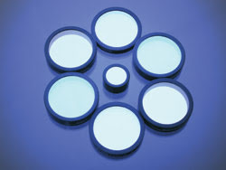
These six 1-in.-diameter optical thin-film filters for fluorescence applications surround a smaller, 10-mm-diameter filter.
• Laser systems. Laser mirrors require low-scattering coatings with high laser damage thresholds. Traditionally they have been made using coating technology limited to about 20 layers. Newer deposition technologies such as ion-beam sputtering allow many more layers. Combining this capability with sophisticated designs and control over the deposition processes can produce mirrors with exceptionally broad spectral and angular bandwidths.
A laser mirror is now available that provides greater than 99 percent reflectivity over wavelengths from 350 to 1100 nm, for any polarization and from 0 to 50° incidence. This all-in-one mirror can replace three or more traditional high-performance, broadband laser mirrors for applications in multiline laser systems (such as Nd:YAG systems that utilize the fundamental at 1064 nm and second and third harmonics at 532 and 355 nm), and in multiphoton and harmonic microscopy.
In one example, taken from a biomedical analysis system, scientists are using these mirrors to steer the near-IR excitation light and the visible fluorescence or scattered higher-harmonic light with high efficiency.5
Wide possibilities
The above are but a few examples of how the recent advances in thin-film coating technology have overturned conventional wisdom of what is possible with thin-film filters for a vast array of applications. The impact of this technological breakthrough should continue to be felt in biotechnology and other fields for years to come.
References
1. A. Mcleod (2003). OFC, technical paper ThM1.
2. M. Scobey et al (2002). OFC Proceedings, paper ThC5.
3. G.J. Ockenfuss et al (2002). OFC Proceedings, paper FA8.
4. www.jdsu.com/site/images/products/pdf/GFF_061802.pdf
5. Professor Thomas G. Brown, the Institute of Optics, University of Rochester (private communication).
Meet the authors
Turan Erdogan is chief technology officer and Victor Mizrahi is president and CEO of Semrock Inc. in Rochester, N.Y.