Smaller devices, thinner wafers and low-k dielectrics spell higher performance for semiconductor chips and emerging opportunities for laser processing tools.
Andrew Masters, Coherent Inc.
In semiconductor manufacturing, the drive to pack more functionality into ever-smaller spaces will ultimately fuel more aggressive chip designs, necessitating use of new low-k dielectric materials, wafer-level packaging, increasingly complex device layers and thinner wafers. All of these solutions will advance chip performance — and introduce new problems for the manufacturing process.
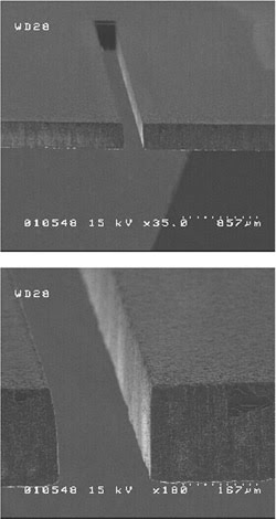
Lasers become more viable machining tools wherever the semiconductor industry implements thinner wafers. These images of a 216-μm-thick silicon wafer, taken with a scanning electron microscope, shows both a laser-cut leading edge and slot (roughly 200 μm). The cutting tool was a 355-nm 7-W solid-state laser operating at a 50-kHz repetition rate.
Conventional chip processing methods based on mechanical saws, for example, could possibly damage chips as wafers thin to below 200 μm. The alternative is to slow the saw feed rate and increase water flow to cool the wafers being diced, but this slows production and increases manufacturing costs. Such issues have fueled interest in the use of solid-state or CO2 lasers to process wafers and next-generation devices.
Besides possible cost benefits, lasers deliver narrower kerf widths and positioning tolerances and eliminate the need for water in the cutting process, an issue that may become more important with the introduction of newer, possibly porous, low-k materials. Their potential extends beyond dicing to micromachining applications ranging from scribing of low-k dielectric materials to drilling of stacked chips. Thermally induced delamination and cracking of the wafer material remain challenges, but such problems have already been resolved in other applications through control of pulse rate, output power and other laser parameters.
Thinner wafers
Wafer thickness generally correlates to wafer diameter. As the industry moved from 200- to 300-mm production, designers made wafers thicker to maintain their mechanical integrity when cut from the silicon crystal. Today, most 300-mm wafers are 720 to 750 μm thick. Several integrated circuit design issues and end-use applications, however, are raising demand for wafers thinner than 200 μm. For instance, the increasing difficulty of reducing transistor size has strained available areal density on memory chips, fueling efforts to stack circuits vertically. Also, the expanding use of smart cards translates to a need to laminate extremely thin layers of circuitry onto plastic cards.
To avoid handling concerns, chipmakers thin the wafer after the integrated circuit fabrication process, which can cause problems when dicing the wafer into chips. Mechanical saws impose higher vibration in thinner, more-flexible silicon, promoting chipping and delamination of devices. Although slowing cutting speed can often minimize wafer damage, this approach is less effective for the thinner wafers and could create a production bottleneck.
Laser dicing and scribing
Where thinner wafers pose challenges to mechanical saws, they provide opportunities for photonic cutting tools; the thinner the wafer, the faster a laser can dice it. Research has demonstrated that lasers can dice wafers less than 150 μm thick faster than saws can. More importantly, wafers of any thickness are processed without damaging the front or back. Lasers also can improve yields and eliminate water cooling, improving cost and performance for devices created on thin silicon. Kerf widths and positioning tolerances are tighter, enabling street widths below 30 μm, instead of the 125 μm or more that is common with mechanical methods. Laser dicing systems also waste less silicon, so chip designers potentially gain more space for patterning.
As chip designs increase in integration and speed, conventional silicon dioxide cannot adequately insulate metal interconnects, prompting chipmakers to use new materials, including those with lower dielectric constants. Low-k dielectrics already are used to reduce capacitance between copper lines, but materials such as fluorinated silicate glass are more fragile than silicate dioxide, and they adhere poorly. As a result, they do not withstand the tensile and shear stresses imposed by mechanical dicing.
At the same time, the industry has also begun implementing wafer-scale or wafer-level packaging, in which chip packages are fabricated on the wafer prior to dicing. Although this approach improves both the cost and the performance of chips, it requires dicing blades to cut through the thick polymer materials of the packages. Over time, these soft polymer materials coat the blade, increasing the potential for damage as processing proceeds.
Unlike saws, lasers can cut through film stacks, polymers and substrates with no mechanical stress on the wafer. They can scribe low-k dielectrics without chipping or delamination, and they can either continue on to dice the wafer or allow a cleaner street for a saw to operate. Lasers also deliver the precision to scribe through single layers, leaving the layers below intact for mechanical dicing. Such scribing operations allow fast, high-yield processing of devices with multiple stacks or brittle materials.
For companies that continue to use mechanical methods, two dicing schemes, both analogous to creating a fire break, use lasers either to scribe trenches on both sides of the saw street or to scribe a single trench that is broader than the width of the blade. The first approach helps prevent polymer materials from loading the saw, which improves its performance and extends its lifetime. But, in either technique, any cracks that are caused during mechanical dicing stop within the borders of the laser scribe.
The LED market is lending further momentum to laser scribing applications. LEDs are grown on high-cost substrates, such as GaAs, sapphire, GaP and SiC, that only grow in value following epitaxy. High-precision saws still dice these devices based on SiC, but blue emitters grown on sapphire have created opportunities for UV laser systems stemming from the hardness of sapphire and the consumable cost involved with traditional mechanical dicing.
In addition, the market for cell phones and other compact electronics demands smaller devices to populate high-density packages. As circuit boards decrease in size, and as phones, for example, increase in functionality, chip manufacturers are looking to stack chips vertically in three-dimensional packages. This approach requires development of through-chip interconnects, which will ensure that the chips in the stack are compatible and of like size. Producing these interconnects in silicon entails a plasma etch procedure combined with photolithography, both of which tend to be slow and expensive.
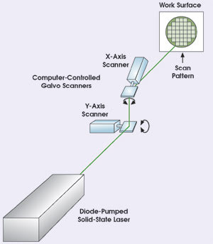
Lasers, however, can drill hundreds of microvias per second and can process a wafer in less than 10 minutes. Besides the cost savings, laser drilling can create holes with 35:1 aspect ratios and, as with laser scribing, can be tuned to leave the layers below intact. With the addition of scanning optics and beam delivery, a single laser can drill microvias of different diameters on the same wafer.
These capabilities also lend themselves to ink-jet printer manufacturing. As consumers transition from traditional film to digital cameras, they have increased demand for higher print resolution. Today’s photographic-quality print cartridges deliver 4800 × 1200 dpi, requiring cartridges to fit over 1000 nozzles per head and to deliver up to 40,000 drops per second onto the print medium. Ink is delivered to the nozzle through a slot machined into the silicon substrate, a process currently performed by mechanical tools with poor process control. Laser drilling tools can offer not only better process control and less chipping along the slots, but also increased throughput and lower operational costs.
Laser types
Silicon absorbs both IR and UV energy so, in principle, both CO2 and tripled solid-state Nd3+ lasers can dice wafers. CO2 laser sources deliver average powers up to 500 W and, compared with diode-pumped solid-state sources, offer more power at a lower cost per watt. Although this enables very high cutting speeds, the 10.6-μm wavelength of CO2 lasers can produce very high thermal damage. These sources can create 100-μm features in silicon, but postprocessing is usually necessary to deal with thermal damage and ejected material. This, however, is acceptable for some applications, such as resizing wafers, because the trimming takes place at the beginning of the production cycle. Afterward, wafers are cleaned and etched, removing any trace of thermal processing incurred by laser processes.
Silicon absorbs both IR and UV wavelengths, but UV energy imposes less thermal damage. Most applications rely on a scanned Gaussian beam from a tripled solid-state laser.
Tripled solid-state Nd3+ lasers cannot match the output power of CO2 sources, but that has become less of a drawback as wafers become thinner. The 10-W average power at 355 nm produced by a diode-pumped solid-state laser — for example, Coherent’s Avia 355-X — is more than adequate to cut 200-μm-thick silicon quickly and with little peripheral damage.
As a rule, optical absorption depth decreases dramatically with wavelength, which means that silicon’s surface absorption of 355-nm photons is much higher than those from a CO2 source. This translates into more efficient coupling, less thermal damage and a cleaner, narrower cut. Further improvement is gained by increasing the repetition rate, typically from 60 to 100 kHz, and lowering pulse energy.
UV beams also provide the benefit of smaller kerfs to dicing operations and improved aspect ratios to drilling processes. Scribing applications, however, have to create comparatively broad trenches, which require multiple passes with a Gaussian 355-nm beam. The irradiance profile of such a beam is typified by so-called “tails,” which can impose thermal damage beyond the beam’s target region. Using optics to create a top-hat profile eliminates their influence.
For years, LED manufacturers have applied 248-nm output from KrF excimer lasers to scribe high-value wafers, despite the need to use photomasks. Frequency-tripled solid-state lasers emitting less than 5 W of 355-nm radiation with pulse energies of 0.1 mJ and at repetition rates of 50 kHz have introduced simpler beam-scanning techniques. Recently, by quadrupling similar lasers that emit less than 3 W at 266 nm, it was proved that even more rapid processing speeds are possible despite lower average powers.
The market for highly functional and compact electronics is driving semiconductor manufacturers to produce smaller devices on thinner wafers and with new materials. These challenges, in turn, have driven chipmakers to seek new tools to maintain low manufacturing costs and high yields. Laser micromachining increasingly presents a solution to cutting, dicing and scribing of microelectronic devices built on silicon and similar substrates, particularly as new chip and package designs emerge in the next decade.
Meet the author
Andrew Masters is business development manager for microelectronics and micromaterials processing at Coherent Inc. in Santa Clara, Calif.