The ability to tune the spectral response of devices is giving component designers more flexibility in application areas from digital imaging to biotechnology.
Peter Wierer, Unaxis Optics
Today a typical thin-film device consists of a multilayer stack of alternating high- and low-index dielectric films, each with a typical thickness of 50 to 100 nm. The number of layers depends on the application and can easily exceed 100. Filters are just one of many components to benefit from the continuing trend toward more-precise multilayer coatings, as well as coatings with fewer layers but added functionality. Other examples can be found in markets ranging from projection display and digital imaging to biotechnology and automobiles.
The most common coating technologies for optical thin films remain conventional electron-beam processes. However, end users should expect to see an increase in specific coating applications that use sputtering, where material is atomized through plasma ion bombardment. Consider color filters, for example, which are used in projection systems. In these devices, an undesirable color gradient can arise in projected images as a result of varying angles of incidence at the color separation mirrors. Color filters produced with sputtering provide compact coatings as well as narrow edge tolerances, high transmission and reflection factors.
The increased density of the optical films produced virtually eliminates the temperature-induced spectral shift associated with electron-beam coating techniques. In addition, emerging optical monitoring schemes are allowing an extremely high level of run-to-run repeatability.
Digital projection and imaging
Sputtering techniques also will gain favor in digital projection technology, such as projection television based on microdisplays with color management systems. In these systems, which are just arriving on the commercial scene, increasing flexibility in coating design has helped boost the image quality specifically in the areas of color and brightness. In addition, the narrow spectral tolerances and stability of optical films reduce UV and IR damage of sensitive components, which should lengthen projector life.
The imaging market using optical thin films basically divides into two segments: devices taking a picture, including those based on CCD and CMOS sensors, and devices making a picture, which include systems that are based on liquid crystal on silicon and optical microelectromechanical systems.
In both segments, the semiconductor-based sensors require a cover glass for packaging reasons. Coatings must enable technologies or increase their quality. The cosmetics of these coatings are most critical, as they are placed very close to the image plane of the device and the miniaturization of pixels is driven to the limits. Typical pixel size is around 4 to 15 μm and should continue to drop — for example, to 2 to 3 μm for CCD sensors. The defect level of the coated lid needs to be in a similar range.
Coating developments must keep pace with the rapid deployment of new technology in these imaging areas. CCD and CMOS sensors, in particular, are sensitive in a broad wavelength range from the UV to the near-IR. The production of high-quality digital images requires a carefully balanced spectrum of visible light to illuminate the imager. Blocking of near-IR radiation is crucial because radiation outside the visible wavelength range does not contribute to the image and, in fact, even degrades it. In addition, as pixels shrink and image resolution increases, defect reduction becomes a critical control factor for camera manufacturers to reduce both costs and physical size.
In these applications, near-IR thin-film blocking filters serve a dual purpose — that of the imager cover and an IR blocking filter. By depositing multiple layers of dielectric materials on the glass substrate, it is possible to produce near-IR blocking filters with steep transitions. Optimizing the filter edge location improves the signal-to-noise ratio, color balance and, ultimately, the image quality. In this case, as in others, it also is becoming easier for designers to tune the spectral response of the components to their design goals. This trend should only continue.
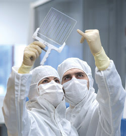
Production of biochip substrates in the cleanroom at Unaxis requires extremely low defect processing for superior performance.
Biotechnology is one of the fastest-growing areas to benefit from optical thin films. Biochips, for example, allow a highly parallel analysis of tissue sample, whole blood or serum in an application where thousands of genes or proteins can interact on-chip with the sample. In some cases, the genes or proteins are deposited on a substrate in a checkerboard pattern with micron-size features.
Some analysts predict that this market, estimated at roughly $800 million US in 2003, will grow to a multibillion-dollar market by 2006. Primary applications are in medical research, drug development and diagnostics.
Thin-film coatings made of dielectric and metallic materials, as well as photolithographic nano- and micro?structuring techniques, will enhance biochip performance. The films are used for evanescent wave sensing where light is captured in a thin film and extends in the surrounding media above the film. Using fluorescence tagging of genes or proteins, detection sensitivity can be boosted by up to 100 times using thin films.
Meet the author
Peter Wierer is business development manager for Unaxis Balzers Ltd. in Balzers, Liechtenstein.