The technology advances signal amplification but has its own limitations.
Murad Karmali, The Cooke Corp., and Dr. Gerhard Holst, PCO AG
A recent advance in CCD technology is the introduction of electron multiplication or charge carrier multiplication CCDs. This technology is effective in applications requiring high light sensitivity, high spatial resolution and reasonably high frame rates at either short or long exposure times. However, the devices may not prove superior to intensified CCDs when it comes to applications that need extremely short exposure times.
Electron multiplication CCDs use a conventional readout-node amplifier design but apply gain to the signal prior to readout. The benefit is an increase in the magnitude of signal charge being digitized at the same readout noise (Figure 1). For applications that are time-sensitive or that suffer from phototoxicity, such as live-cell or ion imaging, the ability to amplify the signal by maintaining a low exposure time is beneficial. Traditionally, this has been accomplished by using intensified CCD cameras, which also amplify signal but at the cost of image degradation and reduced dynamic range caused by various noise sources.
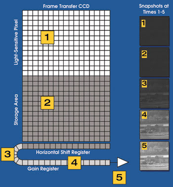
Figure 1. An example of one type of electron multiplication CCD architecture illustrates the sequence of image transfer and the effect of on-chip gain on a very low light image.
Frame-transfer architecture
However, it is incorrect to assume that electron multiplication cameras can entirely replace intensified CCDs. Clearly, for exposure times of less than 1 ms, the latter still have their niche in that they offer pico- to nanosecond resolutions without the image smearing that can be a drawback to electron multiplication CCDs because of their frame-transfer architecture.
Frame-transfer CCDs require the captured image to be shifted under a mask, usually the same size as the active image area and physically located above the active image area being captured. The time required for this transfer depends on the vertical shift time and can vary with manufacturer. As an example, the TX285SPD electron multiplication CCD from Texas Instruments of Plano, Texas, has a 1-MHz vertical shift rate, resulting in a 1k × 1k image that takes 1 ms, which also defines the usable minimum exposure time for a full frame. It is important to realize that the rows closest to the mask will be integrated for a shorter time than those farthest away. However, one can expose a few lines closest to the masked area to enable much shorter exposure time — at the sacrifice of resolution.
With the modified readout node mentioned above, the CCD gain can be adjusted via software to reach the desired level. This results in the amplification of a low signal so that it is resolvable or so that it increases the effective signal-to-noise ratio.
As an example, if the application produces 1000 e– of signal charge per pixel and the readout noise is 20 e–, the signal-to-noise ratio in a conventional CCD would be approximately 50:1. If one amplifies the charge by 20 (20,000 e–), the signal-to-noise becomes 1000:1, or 20 times higher. There are some other sources of noise that haven’t been considered, such as “gain” noise, but they are far smaller than the read noise. Therefore, the device can be used both as a conventional CCD without gain for higher light levels or with gain for higher sensitivity.
Two manufacturing approaches
E2v technologies of Chelmsford, UK, and Texas Instruments have taken different approaches to making these CCDs. Both claim to have pioneered the technology and both continue to offer improved products for the scientific market. Most of the e2v sensors feature larger pixel sizes, allowing 12- to 16-bit digitization, whereas the newer sensors from Texas Instruments feature reduced pixel sizes for higher resolution and 12 to 14 bits of dynamic range. The company’s older chips have a dynamic range of up to 8 bits.
The reduction of dark current noise also is important with these sensors. As with any CCD, cooling reduces thermal noise, but the degree of cooling required depends on the application. If the application demands short exposure times — from milliseconds to just a few seconds — the camera does not need to be deeply cooled; usually –15 to –20 °C absolute is sufficient. If the application requires many minutes of integration, deeper cooling is advantageous.
The key is to refer to the camera manufacturer’s dark current noise specification (typically in e2 per pixel per second) and to multiply this by the seconds of integration time required. The result should then be considered vis-à-vis the acceptable signal-to-noise ratio for the application. This quick calculation helps determine whether investing in a deeper cooled camera is necessary when the application may be the limiting factor.
Applications that benefit from this technology are primarily in the life sciences, such as in live-cell, intracellular-ion, single-molecule and four-dimensional imaging, and spinning-disk confocal and total internal reflection fluorescence microscopy. The success of electron multiplication CCD cameras in the life sciences is attributable to the growing need for higher sensitivity at reduced exposure times to study cell or molecular dynamics.
The CCDs also are used in areas such as surveillance, night vision and x-ray imaging. Although the criterion for higher sensitivity at shorter exposure times is necessary in most physical science applications, the inability to use this technology at submillisecond timescales is a hindrance.
Recent improvements in electron multiplication CCDs include higher-quantum-efficiency front-illuminated sensors (up to 65 percent), back-illuminated sensors with up to 95 percent quantum efficiency and higher readout speed (up to 30 MHz, resulting in 1k × 1k pixels at 30 fps). Future improvements will include higher speed readouts at reduced resolutions for high frame rates — ideal for kinetic applications that do not require much resolution — and larger format arrays. There is also the potential for reduced sensor costs, driven down by volume in surveillance and night-vision applications.
Meet the authors
Murad Karmali, vice president of sales, is responsible for the scientific imaging product group at The Cooke Corp. in Auburn Hills, Mich.
Gerhard Holst is head of the research department at PCO AG in Kelheim, Germany, parent company of Cooke.