The high-volume future of diode lasers rests on partnerships with customers, standardization and efficient manufacturing.
Franck Leibreich, Spectra-Physics Diode Laser
The first semiconductor lasers were produced in the laboratory in the early 1960s. Just months after their development, they were available for sale, their reliability and efficiency generating interest in the marketplace. Of course, the design and the manufacturing processes were immature, so this promising technology came at a stiff price: several thousand dollars for less than a milliwatt of power. Furthermore, they were not always reliable.
Forty years of development have improved our understanding of the basic physics underlying lasing in semiconductors, and have produced advances in materials and diode design. But the prevalence of laser diodes today owes just as much to the optimization of design and manufacturing processes. You can buy diodes now in the range of $10 per watt, and leading manufacturers offer devices with mean time to failure in excess of 100,000 hours.
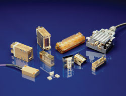
Laser diodes come in all shapes and sizes, including single emitters, bars, stacks and fiber-coupled units.
If diode laser manufacturers can address the remaining standardization and fabrication hurdles, diode lasers could soon find their way into new consumer products for homes and automobiles.
Cost and reliability
Design improvements have lowered costs, and process improvements have increased yields, but the marketplace remains split. Some applications (e.g., industrial manufacturing) need high reliability, and others (e.g., consumer, medical and automotive applications) are more concerned with cost.
The inherent reliability and efficiency of laser diodes, along with the reduced costs concomitant with design and process improvements, have driven their acceptance as excitation and pump sources for solid-state laser design. Diode manufacturers produce thousands for this application each year.
But producing today’s diodes carries new challenges. Having methodically addressed the issues of lifetime and quality, manufacturers now pursue cost points low enough to bring diodes directly to consumer applications.
Device designers find that proving the capabilities of a new laser diode and its suitability for an application is only the first step along the path to making the product available at a reasonable cost/performance point. Manufacturers must carefully evaluate market drivers:
• What characteristics will their customers demand?
• How can we streamline the manufacturing process flow and minimize manufacturing costs while meeting customer specifications?
• How can we efficiently use manufacturing technology?
Increasingly, the answers to these questions have pointed to investments in the latest semiconductor equipment, such as larger-diameter wafer production and process automation, driving up capital costs and threatening the price points manufacturers have worked so hard to achieve.
Lack of standardization
The practice in the laser industry has been to produce custom designs. Even in situations where standardization might be possible, such as with diode laser pumps for solid-state lasers, customers have developed unique specifications for operating point, pulse format, and spatial and spectral brightness.
The traditional 808-nm wavelength used for pumping neodymium-based sources is being supplemented by diodes at additional pump wavelengths, such as 880, 915, 940 and 976 nm. With users demanding unique specifications for relatively small volumes, standardization has been difficult to implement. But without standardization, it is difficult to achieve efficiency in design and process technology.
If it is hard to standardize in this narrow market space, the markets of digital graphics, medicine, materials processing and defense also pose challenges.
With steady growth in unit demand, customers need dramatic reductions in price points, but the fundamental chicken-and-egg problem remains. High-volume, more-standardized production would enable dramatic reductions in cost while maintaining or improving performance, but until price-performance ratios change dramatically, the hoped-for applications that could use those millions of units per year cannot emerge.
So diode manufacturers must decide whether to gamble on these applications and make the equipment and process investments they will require. Manufacturers who do make these investments must partner with appropriate customers, working together in the design phase to optimize and standardize the product.
Path to high volume
Progress toward a de facto standard among device designers could be another way to help diode suppliers gear up more readily for the changes ahead. Perhaps the closest thing to an industry standard is the 1-cm bar, a monolithic array of individual, electrically parallel, broad-area emitters that serves as a cost-effective source of power.
Even this standard product, however, represents a huge family of bar configurations. Laser makers offer bars with different numbers of emitters or different emitter width, or even with a unique bar width and cavity length. Similarly, the devices are available in different packages, with conductive or active cooling. Beam delivery changes from device to device as well, with options such as single-fiber, multifiber or free-space coupling. The high degree of customization rises from application requirements and end-user integration constraints; it endures because of market competition between innovative designs and entrenched technologies.
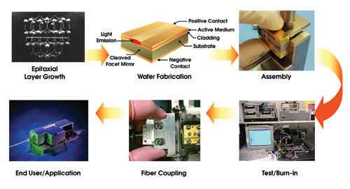
Diode laser production requires a combination of manual and automated processes. Optimizing each step to meet customer requirements is the first step toward high-volume manufacturing.
Standardization does not come naturally to this environment, but with end-user partnerships, the benefits could be significant. Developing efficient fabrication tools and labor utilization is the key to optimizing yields and, hence, to reducing manufacturing costs; standardization would increase the opportunities in this area. An industrywide initiative could accelerate change.
Selecting fabrication tools
Intelligent selection and qualification of manufacturing tools is another key ingredient in cost management. For epitaxial growth, diode laser manufacturers use molecular beam epitaxy and metallorganic chemical vapor deposition to produce devices with interchangeable performance characteristics.
For volume manufacturing, the latter method offers some advantages. One is in serviceability and process capability. Molecular beam epitaxy reactors typically require regular days or weeks for programmed maintenance, with additional significant downtime for nonroutine repairs. This would be unacceptable to a high-volume customer. In contrast, metallorganic chemical vapor deposition servicing can typically be accomplished in one day, with far less downtime. The growth uniformity, growth-rate stability and repeatability from wafer to wafer are also superior with vapor deposition tools.
And while the silicon industry has progressed to 12-in.-diameter wafers and the resulting economies of scale, the diode laser industry continues to use mostly 2- and 3-in. wafers because of the low manufacturing volumes required (annual shipments of well below 1 million bars). The fabrication tools in use are often two or more generations behind state-of-the-art, which limits automation options. Moving even to 4-in.-wafer-production could bring significant automation capabilities.
Unique processing needs
Making use of more-modern silicon semiconductor manufacturing technologies would be useful, but some critical laser diode manufacturing steps have no equivalent in the silicon world; without standardization, they represent a requirement for strong process knowledge and experience. For example, before die singulation, wafers undergo patterning and deposition of dielectric and metal layers (to direct current flow), wafer thinning (to facilitate die singulation through a scribe-and-cleave process) and sintering (to minimize contact resistance).
Another process unique to diode laser manufacturing is stacking and unstacking bars for facet coating immediately after die singulation. Manufacturers typically use manual stacking, alternating laser bars with spacers to control the deposition of the dielectric coating material while facilitating the separation of bars after coating. Automating this process would improve yield and quality and perhaps reduce inspection needs for the final product, but it would require custom tools.
Die attach is also a critical factor in device performance, and optical, mechanical and electrical interfaces all potentially influence assembly yield.
Finally, manufacturers must assure the performance characteristics of finished devices, traditionally by testing each part. With standardization and the concomitant improvements in process control, they could reliably qualify entire production lots. Qualification is nontrivial but often overlooked, given the inherent difficulty of wafer-level characterization of edge-emitting diode lasers and the cost associated with lot sampling. To achieve high yields for wavelength-specific applications such as pumping, manufacturers generally must maintain wavelength uniformity of ±1 nm across a wafer.
Sharing risks and rewards
High-volume applications are the bright future of unmounted diode bars, whose design will have to be optimized for manufacturing capability. Moving to 4-in. wafers and optimizing processes with more automation will reduce costs to a price point that will further drive volume applications to the need for automation of all wafer- and bar-handling steps, and a move from 100 percent inspection to lot sampling.
High-volume opportunities will also allow suppliers to achieve manufacturing economies that will flow down to lower-volume products that otherwise might not see such savings for many years.
So far, market forces have not been strong enough to drive manufacturers to optimize their processes for high volumes, but the path ahead will require close collaboration between volume customers and suppliers where there is shared risk and a shared commitment to design optimization.
OEM customers and those looking to implement lasers in volume applications should partner with manufacturers early in the design process to ensure that their designs can take advantage of these new capabilities.
Meet the author
Franck Leibreich is marketing manager at Spectra-Physics Diode Lasers in Tucson, Ariz.; e-mail: [email protected].