Photonics Spectra Editors
The creation of nanodots, or small islands of a few atoms, offers significant interest to semiconductor laser manufacturers. Compared with quantum well designs, the smaller structures provide electron carrier confinement with increased output tunability and lower thresholds. A new process suggests that lasers can form such nanostructures on metals.
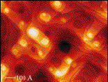
A scanning tunneling microscope shows the formation of pyramidal, nanoscale structures on a copper substrate.
Lasers have become more common in materials processing. However, optical excitation of metals and other materials can result in adverse effects caused by melting thermal and stress on the material's surface.
During experiments that focused different colors of light on copper single-crystal substrates, researchers at the Commissariat à l'Energie Atomique Saclay discovered an electronic photophysical interaction between the light and the copper crystal.
When subjected to pulsed green laser light in the nanosecond regime, in ultrahigh vacuum and at a static temperature of 90 K, adatoms and vacancies formed.
When the temperature was increased to 300 K, the adatoms and vacancies formed nanoscale pyramids. This method could be used to grow nanodot structures for photonic devices, according to researcher Hans-Joachim Ernst.
The green light stimulated electron excitation long enough for it to couple to nuclear motion. Normally, in metals, the excited state lasts only tens of femtoseconds, not long enough for an electron to couple to the atomic motion in metals. "Apparently this is not the case for the copper surfaces," Ernst said.
The group used an Nd:YAG laser from Quantel SA of Les Ulis, France, to produce 10-ns top hat pulses focused to about 2.75 mm. "The beauty of these experiments is that you really do not need some fancy laser," Ernst said.
Although molecular beam epitaxy can grow nanodots on materials, lasers are simpler to work with, he said. Also, by using interference patterns, the structures could be grown in orderly patterns for optical devices.