Demand for smaller, high-quality devices is driving development of chip improvements.
Paolo Vasta, Eastman Kodak Co.
Although CCD sensors had been the technology of choice for imaging devices for years, CMOS-based sensors have emerged as a viable alternative. CMOS sensors offer a number of intrinsic advantages relative to CCDs, including low power consumption and the ability to integrate system functions — timing and image processing, for example — directly on the chip. They have suffered from imaging performance that lags in comparison with what is available from CCDs, but advances in their design have improved the technology’s imaging capabilities dramatically — a development that has significance for the consumer electronics market.
CMOS technology offers a number of benefits that electronics manufacturers can leverage to improve device design, meet specific consumer needs and differentiate their products in the marketplace.
One such benefit is low power consumption. CMOS sensors require, on average, one-third to one-half the power required by a CCD sensor with equivalent resolution. Engineers can take advantage of this characteristic in a number of ways for their products, such as by using smaller and less expensive batteries, or by incorporating brighter liquid crystal displays, stronger flashes, faster digital signal processors, or features such as wireless fidelity, called Wi-Fi, or Bluetooth connectivity.
Another advantage of CMOS sensors is that the entire signal path — from captured light to processed digital signal — can be integrated on the chip. This capability means that additional support chips for system timing or voltage generation are not needed, that fewer and less costly components can be used, and that easier design and more simple printed circuit board layouts become possible, giving more freedom to designers and enabling faster design cycles.
Also, at VGA resolution, CMOS sensors can easily run at 30 fps or faster, and at 3- to 5-megapixel resolution, 5 to 15 fps is achievable while keeping power consumption down. This enables algorithms such as autofocus, autoexposure and automatic white balance to achieve a faster convergence, thereby providing a quicker, more responsive camera. Higher frame rates also mean reduced blur and, in certain cases, enable designers to eliminate mechanical shutters.
Lastly, operations such as frame cropping, zooming, panning and resizing can be done directly on a CMOS sensor, rather than on external support chips. This can help designers simplify software design, free up digital signal processor power and reduce power consumption.
Many of these benefits lend themselves to the design of consumer devices. This is essential because market expectations are placing new demands on electronics. For instance, mobile phones have limited power availability and must divide battery power among several functions. Phone design also imposes constraints on the overall thickness of the device’s imaging module. Similar pressures, such as that to miniaturize, are driving innovation in other devices, such as digital still cameras.
A question of image quality
Despite these strengths, image quality remains a dominating factor for electronic imaging devices and has been a key barrier to the widespread adoption of CMOS technology for digital still cameras. Consumers expect low-end cameras to provide images comparable to those captured with film cameras, and they increasingly expect the images captured with camera phones to have a quality that is comparable to those captured by digital still cameras. The challenge for designers of image sensors is to design systems that meet these consumer expectations without driving up costs.
Designers have explored a number of approaches to image-quality improvement. However, only two — enhancing the fundamental design of the pixels in the sensor array and combining, or “binning,” pixels — are known to improve the quality of low-light imaging, offering the market CMOS sensors with CCD-level performance at a fraction of the cost.
Several photodiodes and array architectures currently are used for CMOS image sensors, the most common of which is a standard architecture that incorporates three transistors into each imaging pixel (a 3T design). This architecture is optimized for both cost and yield, but it suffers from high dark currents, typically of about 1 to 2 nA/cm2. Although this might be acceptable for brightly lighted scenes, it does not allow the sensor to deliver high image quality under low-light conditions.
More recently, the use of a four-transistor (4T), pinned photodiode active pixel has become a feasible and cost-effective solution with good yields. Under this architecture, quantum efficiency increases greatly, and noise can be significantly reduced compared with the 3T design (on the order of hundreds of picoamps per square centimeter). Use of a controlled charge transfer also permits the implementation of a true correlated double sampling at the pixel level, greatly reducing reset noise.
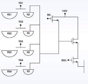
Figure 1. In the 4T4S chip architecture, a cluster of four pixels shares seven transistors and a single amplifier. TG = transfer gate; VDD = amplifier voltage supply; FD = floating diffusion; PD = photodiode; RG = reset gate; RSEL = row-select inputs.
These improvements come at a cost, however, as the use of four transistors instead of three reduces the fill factor of the pixel. The solution is to implement a shared architecture of power lines, signal readout bus lines, and select and reset lines. By doing this, the same noise benefits are realized without a significant reduction in fill factor. An example of such a 4T4S (four transistor, four shared) architecture with pinned photodiodes, where seven transistors and a single amplifier are shared across a four-pixel cluster, yields an effective density of 1.75 transistors per pixel (Figure 1).
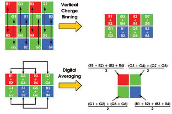
Figure 2. Neighboring pixels of the same color can be combined through initial charge binning, followed by horizontal averaging. This provides imaging withreduced resolution but higher capability in low-light environments.
Besides significantly increasing the image quality available from this design, this shared-pixel architecture provides the opportunity to combine pixels in the charge (rather than in the voltage) domain, trading image resolution for an improvement in overall signal-to-noise ratio. Neighboring pixels of the same color can be combined, first through charge binning (G1 + G2, G5 + G6) and then by horizontal averaging (Figure 2), producing a reduced-resolution image with enhanced low-light sensitivity as well as with lower noise and fewer artifacts than are realized via image decimation (Figure 3).
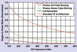
Figure 3. Compared with standard 3T architecture (orange), 4T4S architecture (blue) offers an increased signal-to-noise ratio. It also provides the opportunity to bin pixels for an additional increase in the ratio (green and red).
Similarly, all four pixels associated with a given amplifier can be simultaneously binned and horizontally averaged with three adjacent shared pixels, generating a 4 × 4-pixel monochrome “supercluster.” Although this reduces overall image resolution by a factor of four, the very high sensitivity available in this monochrome-only mode of operation offers new opportunities for camera usage and user benefits.
Benefits of binning
The overall sensitivity increase arising from the 4T, pinned photodiode design is applicable in many markets. However, the enhanced sensitivity available from pixel binning offers opportunities for enhanced functionality in digital still camera applications.
With binning enabled, for example, the sensitivity of the sensor is increased, allowing the camera user to trade image resolution for enhanced operation under low-light conditions. This enables faster shutter speeds (reducing image blur) and allows more images to be captured under natural light conditions.
Another opportunity lies in modern megapixel camera designs, where system resolution must be reduced to video-level resolution to enable video capture. Charge binning allows the resolution to be reduced in a way that increases the overall system sensitivity.
Also, the electronic viewfinder can be improved. By enabling charge binning for live images displayed on a camera’s electronic viewfinder or display, an end user can properly frame the subject of an image under low-light situations; for example, when an external light source or assist lamp is not available.
Lastly, with the added sensitivity available from charge binning (particularly when four pixels are combined to provide a very high sensitivity mode of the camera — see the red line in Figure 3), contrast-based passive autofocus algorithms can converge faster and provide a focus lock without the need for assist lamps or active autofocus systems.
The benefits of implementing modern CMOS image sensor designs in consumer devices go beyond improvements in image quality to include benefits throughout the entire system design. For example, device battery life can be improved, not only because CMOS image sensors require less power, but also because binning can help reduce the need for flash, enable lower-power flash, increase liquid crystal display brightness or reduce digital signal processor intervention to remove noise in low-light snapshots.
System design also is improved by CMOS sensors, while reducing overall manufacturing costs. And the user experience is enhanced, not only by the device’s longer battery life, but also through photographic improvements such as reduced image blur, faster camera response, and better framing, focusing and low-light imaging.
For these reasons, CMOS technology is poised to provide consumer electronics manufacturers with compelling design options, enabling innovations across a number of mass-market consumer applications.
Meet the author
Paolo Vasta is an applications engineer with the Image Sensor Solutions group of Eastman Kodak Co. in Munich, Germany, where he focuses on the use of CMOS imaging devices for mobile and consumer applications; e-mail: [email protected].