Optical approaches are under development to address the problem of switching capacity in the data network.
Pietro Bernasconi, John E. Simsarian, Jürgen Gripp, Markus Dülk and David T. Neilson, Bell Labs
When we surf the Internet or when some of us place a phone call — and in the near future when we watch TV — we send and receive information from the data network (Figure 1). It is a nontrivial task to manage traffic coming from and going to everywhere, especially when the amount of data involved is so large and is growing so rapidly.
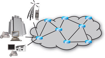
Figure 1. More services are moving to the data network, increasing the pressure on the network nodes.
Network switches and packet routers ensure that all the pieces of information, or packets, are forwarded correctly to their intended destination. Switches and routers receive the data packets carried by the optical transport systems and turn them into electrical signals for processing. The packets are prepared for retransmission and reconverted to optical signals to be sent over optical fibers to the next switch or router, one step closer to the destination.
The data load doubles roughly every year. The transport infrastructure can easily handle the increase in traffic because it relies on data transmission in optical fibers, each of which can support more than 100 channels that, in turn, each carry 10 or even 40 Gb/s of information.
Optical switching
The problem is that switching capacity doubles only every 18 months. The question is whether optical technologies can lead to routers and switches that are better able to satisfy the surging demand.
In today’s large switches and routers — such as those that process 1 Tb/s, the equivalent of approximately 300,000 MP3 song files per second, or more — a challenge on the hardware level concerns bringing these data packets inside the system and moving them efficiently through the various stages. Generally, a switch or router may be schematically represented (Figure 2). Each optical channel is individually directed to an ingress line card, where the optical signal is converted into an electrical one.
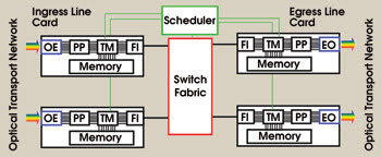
Figure 2. Illustrated is a switch or router architecture. OE: optical-to-electrical signal converter; PP: packet processor; TM: traffic manager; FI: fabric interface; EO: electrical-to-optical signal converter.
The packets are analyzed by a processor that retrieves information such as destination and priority before passing them to the traffic manager. The latter may store the data in memories until a path is available through the switch fabric so that packets can be moved from the ingress card to the desired egress port. There, the data again may be stored for a while before being reprocessed and translated back into optical signals to be sent via fibers to the next network node. The switching operations are supervised by a scheduler — which is centralized or partly distributed across the line cards — that coordinates them so as to maximize the flow across the fabric.
With the rapidly increasing number of lines, the distances between ingress and egress cards also are getting longer in high-capacity switches and routers. Those distances pose a problem because high-frequency electrical signals cannot travel very far without significant radiative losses and signal distortions.
This can be avoided by using an optical switch fabric (Figure 3). The principle of operation is fairly simple. It combines a tunable laser with a prismlike element or diffraction grating. When the wavelength of the laser is changed, the light is sent in a different direction.
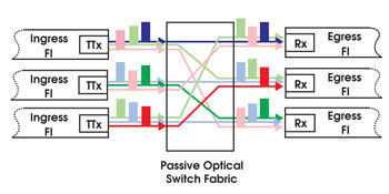
Figure 3. The schematic illustrates an optical switch fabric with tunable optical transmitters (TTx) at the incoming fabric interface (FI) and with optical receivers (Rx) at the output FIs. By selecting the color, each input port can communicate with any output port via a passive optical switch fabric. Telecommunications wavelengths lie within the infrared portion of the electromagnetic spectrum, and colors are used here for illustrative purposes.
With an optical switch fabric, each ingress card contains a tunable laser. The laser is connected to the input of a diffractive element, and the egress cards are arranged at the output side. By selecting the transmitted optical wavelength, each ingress card can be linked to any egress card. These optical links can sustain bandwidths in excess of 40 Gb/s over much longer distances than electrical links.
Both the diffraction elements and the tunable lasers have been demonstrated. The former can take the form of an arrayed waveguide grating (Figure 4), an integrated optical circuit that is functionally equivalent to a conventional diffraction grating.1 Arrayed waveguide gratings with N input and the same number of output ports can be designed so that any input can be connected to any output port by means of one, and only one, of N possible optical wavelengths. Furthermore, no two inputs can access the same output with the same wavelength, although the same wavelength may be employed by different input ports to access different outputs.
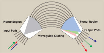
Figure 4. In an arrayed waveguide grating, light from the input waveguides propagates into the first planar region before coupling into the waveguide array. There, as in a conventional diffraction grating, the wavefronts are tilted so that different wavelengths are focused at different locations when the light emerges into the second planar region. If an input port is shifted, the color at the output will move accordingly. The same set of colors can be used simultaneously at each input port without the possibility of color overlap or conflict at the output.
For instance, for N = 40 and with channels modulated at 40 Gb/s, the arrayed waveguide grating can readily handle 160 Gb/s of data, robustly integrated on a few square inches of glass. This data rate can be increased by an additional factor of N to achieve 64 Tb/s if multiple lasers are assigned to each ingress card. In fact, by putting N lasers on an ingress card, the card can be connected to every output at once — so a total of N2 simultaneous connections may be handled by the arrayed waveguide grating.
Because the arrayed waveguide grating provides only passive wavelength routing, the switching is initiated at the transmitter side with wavelength-tunable lasers. Although tunable lasers have been available for some time, the fast tuning speed and the wide tuning range required for a router’s optical fabric have become available only recently. A fast tuning speed is needed to avoid holding back the data while the wavelengths are reassigned, and a wide tuning range is necessary to accommodate as many ports as possible. Tunable semiconductor lasers now offer tuning speeds of a few nanoseconds for switching among more than 100 channels,2 and a proof-of-principle optical switch fabric has been successfully demonstrated in an experiment with each channel carrying data at 40 Gb/s.3
The same optical switch fabric also has been used in a more advanced configuration to show how to expand the switches’ and routers’ capacity to hundreds of terabits per second. Two optical switch fabrics are arranged in front of and after an electronic stage devoted to data processing (Figure 5). In this multistage architecture, data at each input port of the first switch fabric are periodically recolored by the input tunable lasers so that they are randomly directed to and uniformly distributed across the input ports of the second stage, accomplishing “traffic load-balancing.” In the midstage, data are processed and stored in memory until the second optical switch fabric provides a light path from the memory to the desired destination.4
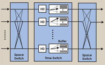
Figure 5. In this three-stage load-balanced architecture, packets at the input ports are alternatively forwarded via a space switch to any port in the second stage. According to their destination, packets are stored in memories (or time switches) from which they are transferred to the output ports via a second space switch running according to a deterministic schedule. HD: header detector.
The natural question is, “Why use two switch fabrics rather than one?”
Easing rush hour
To clarify the operating principle of the three-stage (space/time/space) switching scheme, consider a major road intersection controlled by traffic lights that sequentially allow you to go from one road to another. As long as the traffic is uniform — i.e., the probability that you may want to turn to a specific direction is about the same regardless of the direction and regardless of where you are coming from — the intersection will work just fine. But if at some point (for example, at rush hour) a lot of traffic wants to turn to a specific direction, long lines will form. You may have to wait, even though you would like to turn into a less busy road. To alleviate the problem in the traffic situation, costly and sophisticated “smart” lights and preferential lanes have been implemented.
In the three-stage switching configuration, the intersection is split into two equal and consecutive intersections. So when you come to the first crossing, you simply turn to the direction allowed by the green light, regardless of your destination. Only at the second traffic light do you pick your final road. To do so, you may have to wait, but at this stage, the traffic already has been shuffled, so its distribution is uniform. Therefore, there is no need for “smart” traffic lights or for intricate loops and detours, even during the rush hour.
This simplicity is particularly important for large switches and routers in which the connections between input and output cards are controlled by an arbiter that organizes the overall incoming traffic, manages the memories and synchronizes the transmission at each port to maximize throughput.
Because the traffic between inputs and outputs may change on a short timescale, the arbiter is expected to adapt the router’s configuration rapidly to avoid introducing long delays. The evaluation of a new configuration in a large router is a demanding mathematical task whose computational complexity grows quickly with capacity and eventually may become intractable.
The effectiveness of the three-stage architecture based on the hybrid electrical/optical approach has been verified, with performances that are better than a conventional single-stage switch. However, the increase in performance is accomplished at the expense of additional optical-to-electrical and electrical-to-optical translation stages, which add complexity and cost, especially at higher transmission speeds. Also, data manipulation is performed in almost the same, somewhat awkward, way as in the line cards described earlier.
With the support of a program sponsored by the Defense Advanced Research Projects Agency, investigators at Bell Labs at Lucent Technologies in Holmdel, N.J., are exploring how to reduce the number of conversions and to keep the signals in the optical domain as much as possible. The goal is to replace electronic components with their optically integrated counterparts. For example, fast tunable-wavelength switches are used to change the wavelength on which the data are carried so that the optical traffic flows through the switch fabrics without unnecessary translations.
Fast switches
To this end, an integrated tunable-wavelength switch has been demonstrated in a semiconductor optical chip of millimeter dimensions. The device combines a fast tunable laser and a nonlinear optical element for wavelength conversion (Figure 6). The wavelength of the multifrequency laser is selected by injecting current into a semiconductor optical amplifier. Unlike in many other types of semiconductor lasers, such as distributed feedback and distributed Bragg reflector lasers, the currents do not need to be controlled precisely. This sort of digital tuning can be extremely fast, providing subnanosecond switching speeds.
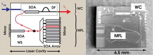
Figure 6. Left: The diagram shows the layout of an integrated tunable wavelength converter (WC). When current is injected into one of the semiconductor optical amplifiers (SOA), a different wavelength is emitted and is sent to the nonlinear optical element via a power coupler. The power coupler comprises an SOA and a delay filter (DF), whose combined action converts the wavelength of the data from λsigto λj using a multifrequency laser (MFL). WS: wavelength switch. Right: The image shows an InP chip with an SOA+DF wavelength converter and a folded MFL.
The laser light then is coupled into the wavelength converter, which consists of a semiconductor optical amplifier followed by a delay filter. The combined action of this arrangement operates as an optical gate that is controlled by the incoming signal λsig. Whenever an input pulse enters the semiconductor optical amplifier, the gate opens and releases a pulse on the new wavelength λj provided by the tunable multifrequency laser.
Physically, the combined action of the semiconductor optical amplifier and the filter can be described as follows: In the absence of the input data at λsig, the delay filter (an asymmetric Mach-Zehnder interferometer) is set so that, at its output, the light at λj interferes destructively, and no signal is released. Whenever an input pulse at λsigenters the semiconductor optical amplifier, the optical phase of λj is modified via nonlinear optical effects. This phase change temporarily pushes the filter from a fully destructive to a constructive interference state so that a pulse at the new wavelength is released.
These wavelength converters make the first and last stages of the three-stage architecture fully optical. But making the middle stage optical still is problematic. The hitch is timing — the storage, or “buffering,” of optical pulses until there is an opening for them in the system. The implementation of an optical buffer remains one of the most challenging tasks, especially if RAM optical storage is required.
Fortunately, the deterministic nature of the scheduling process in the three-stage architecture enables the implementation of the optical buffers in a simple manner. This derives from the fact that the scheduler, or traffic light, draining the buffers is predictable, so that once the destination of a packet is recovered, the time that it will have to wait in the memory is determined independent of the rest of the incoming traffic or from the status of the other midstage memories. Therefore, the memories can take the form of simple, discrete delay lines (hence the name of the second stage: time switch) and can be readily constructed.
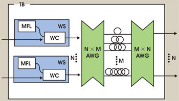
Figure 7. The drawing illustrates an optical time buffer (TB) using a shared set of delay lines whose lengths are a multiple of the packet length. Once the local scheduler has determined the delay, the wavelength switch (WS), which comprises a tunable multifrequency laser (MFL) and the wavelength conversion section (WC), is tuned to the wavelength corresponding to the desired delay. Multiple switches can share the same set of delays. AWG: arrayed waveguide grating.
An effective scheme involves a wavelength converter at the input of an arrayed waveguide grating that addresses the delays by changing their wavelength (Figure 7). A second arrayed waveguide grating then will ensure that the signals launched from an input port will emerge from a unique output port. Because of the wavelength routing nature of the grating, the same set of delays can be shared by multiple inputs, each controlled by a wavelength switch. Each delay line then will hold multiple packets on different wavelengths.
Although this arrangement has been tested with discrete components, efforts are now devoted to its implementation in fully integrated form. To this end, interesting opportunities may reside in the use of so-called “slow light” — novel ways to drastically reduce the propagation speed of light so that much shorter physical distances can provide longer time delays (see “Slow Light: From Basics to Future Prospects,” on page 44).
Once the traffic manager and the memories in the line cards of today’s switches and routers have been implemented optically, the packet processor will be the only component for which optical-to-electrical/electrical-to-optical translation is required — and, therefore, the only component standing in the way of realizing a fully optical switch or router.
The packet processor detects the header and label and, depending on the overall network architecture, may add or remove headers and/or swap labels and addresses. Header recognition can be performed optically by tapping a fraction of the light from the main optical stream to detect the optical information and converting it into the electrical domain, where it can be processed to provide the control of the time buffers.
But, realistically, an all-optical implementation of these header functions may require more elaborate approaches, some of which have been demonstrated in research laboratories.5,6
Meet the authors
Pietro Bernasconi (e-mail: [email protected]), John E. “Jesse” Simsarian (e-mail: [email protected]), Jürgen Gripp (e-mail: [email protected]), Markus Dülk (e-mail: [email protected]) and David T. Neilson (e-mail: [email protected]) are all research scientists with the Photonic Networks Group at Bell Labs in Holmdel, N.J.
References
1. C. Dragone, C.A. Edwards and R.C. Kistler (October 1991). Integrated optics NxN multiplexer on silicon. IEEE PHOT TECH LETT, pp. 896-899.
2. B. Mason et al (July 2000). Design of sampled grating DBR lasers with integrated semiconductor optical amplifiers. IEEE PHOT TECH LETT, pp. 762-764.
3. J. Gripp et al (November 2003). Optical switch fabrics for ultra-high-capacity IP routers. J LIGHTWAVE TECH, pp, 2839-2850.
4. C.-S. Chang, D.-S. Lee and Y.-S. Jou (April 1, 2002). Load balanced Birkhoff-von Neuman switches, part I: one-stage-buffering. COMPUT COMMUN, pp. 611-622.
5. D.J. Blumenthal et al (February 2003). Optical signal processing for optical packet switching networks. IEEE COMMUN MAG, pp. S23-S29.
6. See selected papers in Ultrafast optical packet processing technologies for optical packet-switched networks (July 2004), NTT TECH REV, pp.12-56.