ATLANTA, April 19, 2006 -- A study of how electrons behave in circuitry made from ultrathin layers of graphite – known as graphene – suggests the material could provide the foundation for a new generation of nanometer-scale devices that manipulate electrons as waves, much like photonic systems control light waves.
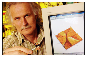
Georgia Tech Professor Walt de Heer holds a proof-of-principle device constructed of graphene. (Georgia Tech Photo: Gary Meek)
Researchers at the Georgia Institute of Technology and the Centre National de la Recherche Scientifique (CNRS) in France report measuring electron transport properties in graphene that are comparable those seen in carbon nanotubes. Unlike carbon nanotubes, however, graphene circuitry can be produced using established microelectronics techniques, allowing researchers to envision a “road map” for future high-volume production.
“We have shown that we can make the graphene material, that we can pattern it, and that its transport properties are very good,” said Walt de Heer, a professor in Georgia Tech’s school of physics. “The material has high electron mobility, which means electrons can move through it without much scattering or resistance. It is also coherent, which means electrons move through the graphene much like light travels through waveguides.” The results should encourage further development of graphene-based electronics, though de Heer cautions that practical devices may be a decade away. “This is really the first step in a very long path,” he said. “We are at the proof-of principle stage, comparable to where transistors were in the late 1940s. We have a lot to do, but I believe this technology will advance rapidly.”
The research, begun by de Heer’s team in 2001, is supported by the National Science Foundation and Intel Corp. In their paper, published April 13 in Science Express, an online advance publication of the journal Science, the researchers report seeing evidence of quantum confinement effects in their graphene circuitry, meaning electrons can move through it as waves. “The graphene ribbons we create are really like waveguides for electrons,” de Heer said.
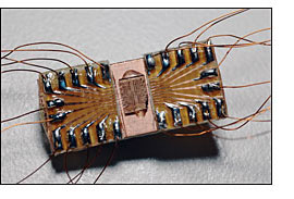
Close-up image showing a proof-of-principle device based on graphene circuitry. (Georgia Tech Photo: Gary Meek)
Because carbon nanotubes conduct electricity with virtually no resistance, they have attracted strong interest for use in transistors and other devices. However, the discrete nature of nanotubes – and variability in their properties -- pose significant obstacles to their use in practical devices. By contrast, continuous graphene circuitry can be produced using standard microelectronics processing techniques, de Heer said.
“Nanotubes are simply graphene that has been rolled into a cylindrical shape,” he said. “Using narrow ribbons of graphene, we can get all the properties of nanotubes because those properties are due to the graphene and the confinement of the electrons, not the nanotube structures.” de Heer envisions using the graphene electronics for specialized applications, potentially within conventional silicon-based systems. “We have shown that we can interconnect graphene, put current into it, and take current out,” he said. “We have a very promising electronic material. We see graphene as a platform, a canvas on which we can work.”
De Heer and collaborators Claire Berger, Zhimin Song, Xuebin Li, Xiaosong Wu, Nate Brown, Tianbo Li, Joanna Hass, Alexei Marchenkov, Edward Conrad and Phillip First of Georgia Tech and Didier Mayou and Cecile Naud of CNRS start with a wafer of silicon carbide, a material made from silicon and carbon atoms. By heating the wafer in a high vacuum, they drive silicon atoms from the surface, leaving a thin continuous layer of graphene.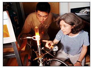
Researchers Xuebin Li and Claire Berger monitor high-temperature graphene growth in an induction furnace. (Georgia Tech Photo: Gary Meek)
Next, they spin-coat onto the surface a photo-resist material of the kind used in established microelectronics techniques. Using electron-beam lithography, they produce patterns on the surface, then use conventional etching processes to remove unwanted graphene.
“We are doing lithography, which is completely familiar to those who work in microelectronics,” said de Heer. “It’s exactly what is done in microelectronics, but with a different material. That is the appeal of this process.” Using electron beam lithography in Georgia Tech’s Microelectronics Research Center, they’ve created feature sizes as small as 80 nm. The graphene circuitry demonstrates high electron mobility – up to 25,000 square centimeters per volt-second, showing that electrons move with little scattering.
The researchers said they expect to see ballistic transport at room temperature when they make structures small enough. So far, they have built an all-graphene planar field-effect transistor. The side-gated device produces a change in resistance through its channel when voltage is applied to the gate. However, this first device has a substantial current leak, the team said, which they expect to eliminate with minor processing adjustments. The researchers have also built a working quantum interference device, a ring-shaped structure that would be useful in manipulating electronic waves, they said. 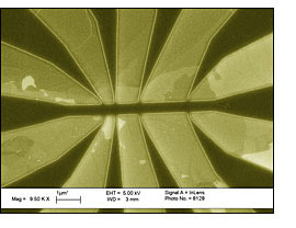
A scanning electron microscope image of a nano-patterned epitaxial ultra-thin film of graphene shows a hall bar structure used to measure transport properties under magnetic fields. (Image: Zhimin Song)
The key to properties of the new circuitry is the width of the ribbons, which confine the electrons in a quantum effect similar to that seen in carbon nanotubes. The width of the ribbon controls the material’s bandgap. Other structures, such as sensing molecules, could be attached to the edges of the ribbons, which are normally passivated by hydrogen atoms. Beyond coherence and high electron mobility, the researchers said that the speed of electrons through the graphene is independent of energy – just like light waves. The electrons also possess the properties of Dirac particles, which allow them to travel significant distances without scattering.
Among the challenges ahead, they said, is improving the techniques for patterning the graphene, since electron transport is affected by the smoothness of edges in the circuitry. Researchers will also have to understand the material’s fundamental properties, which could still contain “show-stoppers” that might make the material impractical. De Heer has seen hints that graphene may offer some surprises. “We already have indications of some new and surprising electronic properties of this material,” he said. “It is doing things that we have never seen in two-dimensional materials before.”
For more information, visit: www.gatech.edu/research