
Optical System Monitors and Controls Thin-Film Stress
Ruth A. Mendonsa
Measuring the stress of thin films as they are deposited is critical for achieving the optical, electronic and mechanical properties required in today's high-performance devices. Controlling the degree of stress can present a challenge, and the unwanted changes in stress that can occur at any stage of the fabrication process can result in performance degradation, interconnect failures and film delamination.
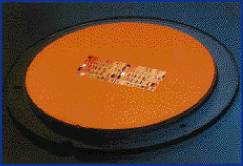
The multibeam optical sensor from k-Space passed the test for monitoring film stress during film deposition on x-ray masks such as this one fabricated at the IBM Advanced Mask Facility. Courtesy of IBM.
Engineers at IBM's T.J. Watson Research Center in Yorktown Heights, N.Y., and the IBM Advanced Mask Facility in Burlington, Vt., are concerned with accurately monitoring and controlling the film stress of refractory metal absorber layers for x-ray mask fabrication. Film stress measurements now are performed after deposition using an off-line system that calculates average film stress from wafer curvature measurements.
Researchers from IBM evaluated k-Space Associates' multibeam optical sensor to determine if it had the sensitivity required to monitor and control the deposition of the absorber layer for x-ray lithography masks. After modification of the optics, which k-Space Associates' development engineer Charles Taylor said is done easily with this system, the company's sensor did the job.
Curvature detection
Taylor said the principles of the multibeam optical sensor are simple: Under stress, a thin film will induce curvature in the underlying substrate. The challenge of the technique is to accurately detect the curvature in the substrate with sufficient resolution to measure the amount of stress typically found in thin films. For very thin films -- on the order of tens of angstroms -- the radius of curvature can be as large as 2 to 5 km.
The system uses stationary optics to produce multiple parallel laser beams. The number and spacing of the beams in the array can be controlled by changing the configuration of the optics. The low-power laser beams are reflected from the sample surface and imaged using a charge-coupled device (CCD) area detector. As the wafer becomes stressed, the curvature causes the beams to reflect to slightly different positions on the detector. The CCD detector simultaneously measures relative change in spacing of all the spots and the data are converted to represent the radius of curvature or film stress.
According to researchers at IBM, the new in situ sensor was capable of detecting film stresses smaller than 2 MPa-µm, which is sufficient to follow the stress evolution during the deposition of films of more than 100 nm and to monitor the uniformity of the stress through the layer.
Published: September 1998