A brick wall looms for electronic clocking, but photonic techniques offer a path to higher speeds.
James P. Siepmann, LightTime LLC
In the fast-paced and ever-changing microprocessor world, there is one undeniable truth: Photonic clocking will happen. It is just a question of when.
The International Technology Roadmap for Semiconductors, which has been accurate in laying out future microprocessor technologies, makes it clear that the electrical clocking technology will meet its demise somewhere between 2008 and 2012, which correlates to clock speeds of about 8 to 10 GHz.1 (The public is particularly familiar with the core clock speed rating of microprocessors, so it is used in this article rather than the local clock speed employed in the Roadmap, which typically is twice the core speed.)
Ticking clock
Because it takes about five years to implement any new technology into high-volume manufacturing processes, the clock is ticking, so to speak, for the industry to make this transition to the next-generation clocking technology.
The move to the photonics approach is driven by three issues: the copper limit, electrical problems and the photonic advantage. The copper limit refers to the fact that no matter how the size, shape or composition of these interconnects (i.e., wires) change, they will no longer be a cost-effective solution much past 8 GHz. No known technologies will extend the performance of copper interconnects to the necessary speeds, regardless of cost.
The electrical problems involve the various phenomena — electromagnetic interference, electromigration, crosstalk, signal degradation —that impose serious limitations on clock speed. Finally, there is the undeniable photonic advantage: Metal interconnects can carry a high-frequency signal only a few centimeters, but optical waveguides can carry them meters or even kilometers before encountering the same level of signal deterioration.
These challenges in microprocessor electronic clocking present a major application opportunity for photonics: high-volume, low-cost laser clocking sources. But what source will be best? Among the several photonics technology options considered below, the passively mode-locked internal-cavity semiconductor laser provides an excellent combination of performance and economy.
Microprocessor clocking currently is achieved by using an accurate and stable time source, such as a quartz crystal, resonating at a low frequency (e.g., 32,768 Hz) and multiplying it to the desired microprocessor clock frequency (e.g., 2 GHz). Although quartz crystals are commonly integrated with 15 divide-by-two circuits to produce a second of time for watches (32,768 = 215), going the other direction to generate gigahertz clocking frequencies for computers is more difficult. Any jitter (variation in signal occurrence) or skew (variation in signal arrival) decreases proportionally as a frequency is divided to obtain the desired value, but the percentage of jitter and skew is also multiplied when a frequency is multiplied.
For instance, if a quartz oscillator has a combined jitter and skew of 1 percent, dividing down to 1 s decreases that combined error to 1/32,768 percent. In contrast, multiplying to 4 GHz increases the jitter and skew by more than 100,000 times, or more than 1000 clock cycles.
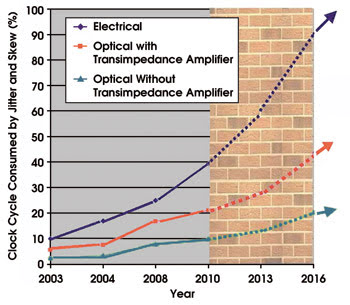
Figure 1. Electronic clocking will hit a brick wall in about four years. Photonic clocking, because its jitter and skew consume a much lower fraction of the total cycle, provides a solution to this dilemma. With a transimpedance amplifier added to the photodetector, photonic-clocking skew and jitter consume an even smaller fraction of the cycle.
Obviously, that will not work, which is why the quartz crystals used in computers have jitter of less than 0.00001 percent. But even using better oscillators and improved designs, about 50 percent of a microprocessor’s clock cycle soon will be consumed by jitter and skew (Figure 1). As Intel Corp.’s platform group noted, clock skew and jitter and latch delay become a much larger percentage of the clock cycle at higher frequencies, reducing the percentage of the cycle that is available for use by actual logic.2 Photonic clocking, on the other hand, still will have most of its clock cycle available for decades to come.
It is difficult to maintain the clock signal’s integrity for much more than 1 cm using metal interconnects. As the clock frequency increases, the viable transmission distance becomes even smaller. With the recent move to multicore processors, however, the distance from a central clock to the individual cores will increase.
Lasers as clocks
Using a clock for each core may sound like an easy solution, but doing so would mean having to compensate for the differences in jitter and skew of each one to enable parallel processing. Besides, using multiple clocks would increase power consumption and heat production, which were the main reasons that the industry went to multiple cores in the first place.
Photonic clocking uses a pulsed laser at the desired wavelength, coupled with a waveguide that distributes the signal to photodetectors. When the optical signal reaches its destination, the photodetector converts it into an electrical signal that is used by the processor at that location on the chip.
Depending on the strength of the laser and on the number of destinations in which its signal is divided, a transimpedance amplifier may or may not be used with the photodetector. (There are advantages to using a photodetector alone, such as less jitter, skew and delay, but eliminating the amplifier requires a more powerful laser clock.)
So what type of laser is best-suited for clocking applications? The answer would be simple if the major microprocessor manufacturers used the same III-V materials from which semiconductor lasers are made, such as GaAs and InP. The lasers then could be built easily and right on the microprocessor chip. These materials are more costly than silicon, but that expense would decrease dramatically in large enough volumes. In fact, most of a microprocessor’s cost is fabrication, packaging, etc.; only a small part is due to the raw materials.
Such a switch would improve performance and offer a myriad of new opportunities. Unfortunately, the major manufacturers already have spent trillions of dollars creating a silicon infrastructure, so they will rely on silicon as long as possible. Moreover, even if the cost of making microprocessors increased only by a couple of dollars per unit, that still would mean a difference of hundreds of millions of dollars annually.
This is why the industry has been trying for years to develop a silicon laser, which may seem like an oxymoron to many because it once was thought impossible to get silicon to lase. Even now, it is a difficult feat at best.
Despite the excitement in the press this past year, silicon lasers are many years from becoming practical devices, and they may never supplant the other laser options that are available. These silicon lasers are basically Raman amplifiers, so they still would need a laser or other powerful light source to get the silicon to lase, a modulator to produce a clock signal and a high-frequency electrical clock to run the modulator; all in all, it is not a simple or inexpensive solution. Using a laser to generate a laser does not make much sense logically or financially.
There have been attempts to dope a silicon laser with erbium so that it can electroluminesce, but this has an efficiency that is about 10,000 times worse than a simple III-V laser. It would take more than 10 W of power to produce just 1 mW of light, with the rest ending up as heat — the bane of microprocessors. Even assuming major improvements in efficiency, silicon lasers likely will be too late for the conversion to photonic clocking.
Acknowledging the necessity for a III-V semiconductor laser is the first step in finding the best photonic clock solution, but it still is necessary to determine the best way to get the laser to give a pulsed output like a “clock” should. Because the laser must be simple and cheap, those that require multiple components or that display high power consumption are eliminated from consideration.

Mode-locked lasers
The most desirable alternatives are mode-locked lasers, which feature output frequencies in the range of megahertz to hundreds of gigahertz (see “Understanding Mode-Locking,” page 86). Although a laser can be actively mode-locked, or externally triggered, this approach requires multiple components, takes up more space and is cost-prohibitive. That leaves passively mode-locked lasers — of which there is a choice between internal- and external-cavity devices.
It may be possible to produce an external-cavity laser as a single component, but they typically are composed of multiple components. Some commercial units cost as much as $50,000 each.
Passively mode-locked internal-cavity semiconductor lasers, however, are the least expensive and easiest to manufacture of the mode-locked lasers. This laser had problems with jitter in the past, but these problems have been solved.3 The lasers are the smallest and simplest photonic clocks available today.
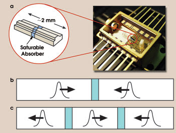
Figure 2. The saturable absorber is a monolithic segment of the passively mode-locked internal-cavity semiconductor laser (a). If the saturable absorber is in the middle of the laser cavity, the output pulse train will be at twice the fundamental mode-locking frequency (b). If the resonator is divided into three sections by two saturable absorbers, the output pulse train will be at three times the fundamental mode-locking frequency (c).
The lasers are standard semiconductors, which cost only a few dollars each, but with the addition of a saturable absorber section (Figure 2a). The absorber forces the photons in the laser cavity to bunch up into a pulse that has sufficient peak power to saturate the absorption — in other words, the saturable absorber mode-locks the laser.
Photonics to the rescue
The placement of the saturable absorber is critical in determining the frequency of the mode-locked pulse train from the laser. If the absorber is placed at one end of the laser cavity, the laser will be mode-locked at the fundamental cavity frequency. If it is placed in the middle of the cavity, the laser will be mode-locked at twice its fundamental frequency (Figure 2b). If the laser is divided into three equal-length sections by two saturable absorbers, it will be mode-locked at three times its fundamental frequency (Figure 2c).
The key to understanding Figure 2c is to realize that two pulses always overlap at the saturable absorber, providing the photon fluence necessary to saturate it. The same concept can be extrapolated to higher mode-locking harmonics: If the laser is divided into N different sections by N–1 saturable absorbers, it will be mode-locked at N times the fundamental mode-locking frequency. (Other design subtleties involving the reflectivity — or lack thereof — of the laser facets are beyond the scope of this article.) Thus, by varying the length of the laser and the number of saturable absorbers, a laser designer can create any stable frequency from a few to hundreds of gigahertz.
In practice, a saturable absorber can be created in a semiconductor laser by fabricating a different material into the structure or by reverse-biasing a small section of the laser. The latter approach obviously is easier and cheaper, and it enables postmanufacture adjustment by tweaking the voltage applied to the chip. This technique also allows straightforward control of the clock speed.
Because there is no physical difference between the saturable absorber and the gain sections, changing the electrical bias of the absorber from reverse to forward effectively turns it “off.” Thus, the output frequency of a laser with multiple absorbers may be changed by turning various combinations of absorbers on and off, which could be used for the slow, medium or fast clock in a microprocessor — today, typically 1, 2 and 4 GHz, respectively.
Passively mode-locked internal-cavity semiconductor lasers have been tested to be within 1 percent of their designed frequency targets. Although no long-term (more than a day) testing has been done, long-term drift could be compensated with the use of a closed-loop thermoelectric cooler. By employing various reflective coatings, the lifetime of these lasers could be extended to make them suitable for operation in heat-intensive environments, such as within a microprocessor. And the new generation of passively mode-locked internal-cavity semiconductor lasers displays low jitter and produces an excellent pulse train (Figure 3).
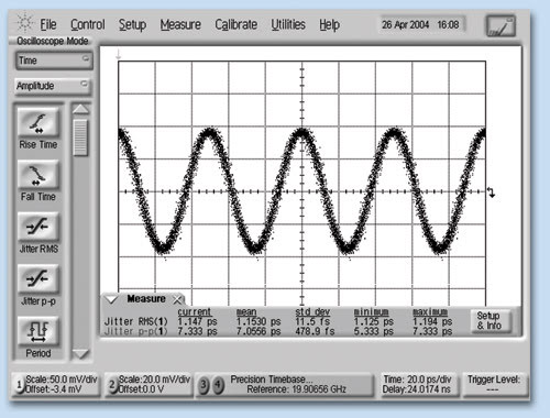
Figure 3. This pulse train occurs at twice the fundamental mode-locking frequency of the AlGaAs passively mode-locked internal-cavity semiconductor laser. Jitter is less than 2 ps rms in this 20-GHz pulse train.
Their wavelength also could be changed by using a different material system. Most testing has involved devices with output wavelengths around 860 nm because they yield the best power efficiency and because these wavelengths can be transmitted through various silicon-compatible waveguides and work with the SiGe photodetectors that are likely to be used in microprocessors.
Photonics is ready to rescue microprocessor clocking. It is one thing to make prototypes and try various mounting and alignment techniques, it is still another to refine them for high-volume manufacturing. Regardless of the chosen laser and method of integration, the development of photonic clocking must start soon to avoid the brick wall ahead.
Meet the author
James P. Siepmann is a founder and chief research officer of LightTime LLC in Oshkosh, Wis.; e-mail: [email protected].
References
1. See the International Technology Roadmap for Semiconductors, 2005 edition, available online at public.itrs.net.
2. G. Hinton et al (February 2001). The Microarchitecture of the Pentium 4 Processor. INTEL TECH J. Available online at www.intel.com/technology/itj/index.htm.
3. J.P. Siepmann and A. Rybaltowski (March 2006). Scalable passively mode-locked semiconductor lasers for microprocessor clocking. Proc. SPIE, Vol. 6115, Photon Processing in Microelectronics and Photonics V, pp. 19-30.
Understanding Mode-Locking
Mode-locking occurs when the photons in a laser cavity bunch up into a pulse rather than spreading out uniformly. The pulse resonates between the ends of the laser, which act like mirrors. Each time the pulse hits a partially reflecting mirror, some of it is transmitted, resulting in an output train of short pulses.
In a passively mode-locked laser, an intracavity saturable absorber forces the photons to bunch. It absorbs the photons unless the instantaneous fluence in the absorber is above a threshold value. The pulse, which builds up as the result of noise, exceeds this threshold and is transmitted through the absorber with minimal loss. Photons not in the pulse are lost in the absorber. The pulse continues to grow until it saturates the gain available from the population inversion. The fundamental frequency (f) of the output pulse train is the reciprocal of the resonator’s round-trip transit time; that is, f = c/2Ln, where c is the speed of light in a vacuum, L is the length of the laser cavity and n is the refractive index of the cavity.
Under conditions that are explained in the article, it is possible for more than one pulse to circulate within the laser cavity. In the case of harmonic mode-locking, the frequency is an integral multiple of the fundamental frequency.
The harmonic mode-locked semiconductor laser is discussed as the source of a photonic clock signal in this article.