
Optical Sensor Monitors Film Growth
Kevin Robinson
Over- or under-stressed thin films means that semiconductor devices, such as quantum well lasers, don't work right. To help remedy this problem, a laser optical sensor, called the multibeam optical sensor, measures stress during a thin film's deposition.
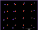
The shift in the reflection of multiple beams allows the multibeam optical sensor to accurately determine the curvature of thin films as they go from unstressed (red) to stressed (blue) conditions.
The device, developed by a collaboration of researchers from k-Space Associates Inc. in Ann Arbor and Sandia National Laboratories in Albuquerque, N.M., uses a diode laser and a series of etalons to split a beam into a pattern of beams that it uses to measure the stress of thin films. The system actually measures the curvature of the wafer underneath the film; no mean feat because the curvature radius of a typical wafer often exceeds 2 km. The beam array is reflected from the film surface and detected by a high-resolution charge-coupled device detector. The system detects changes in the curvature by analyzing changes in the spacing between the reflected beams.
According to Charles Taylor of k-Space, a pattern of beams allows the device to be used in a production environment. Other methods such as laser scanning and interferometry systems cannot be used during production because they are highly sensitive to vibrations as well as to the positioning of the target wafer. The multiple beams detect the surface's curvature much more quickly than other systems, and they are less sensitive to vibrations and sample positioning.
The optical sensor uses a Hitachi diode laser operating between 635 and 670 nm, recently upgraded to a higher-power version to improve the system's flexibility. "The actual power at the sample is in the microwatt range because of the reflective etalons," Taylor explained. Powers that low do not damage the sample, he added.
K-Space is working with IBM facilities in Yorktown Heights, N.Y., and Burlington, Vt., and Motorola in Tempe, Ariz. Taylor said that although the systems are expected to cost about $60,000, customers' needs will dictate the price. He added that the company is working to improve the curvature resolution and design a unit that could warn users about fabrication problems.
Published: September 1998