
Raman Amplifier in Silicon Generates Electrical Power
Photovoltaic effect generates power in an external electrical circuit.
Breck Hitz
In the quest to integrate photonics and electronics in monolithic devices, several laboratories have recently demonstrated silicon Raman lasers (Photonics Spectra, November 2005, p. 52). A fundamental problem inherent in these devices has been optical absorption by free carriers created in the silicon by two-photon absorption. In the first reported silicon laser, the challenge was met by operating the laser in a pulsed mode: The laser pulse came and went before enough free carriers built up to impede it.
Subsequently, other researchers operated the first continuous silicon laser by fabricating a PN junction around the laser. A reverse bias applied across the junction swept the free carriers out of the laser, reducing the free-carrier absorption sufficiently for the laser to reach threshold. However, in this approach, the current of free carriers being swept out generated heat in the junction. Heat is the primary limitation in the design of very-large-scale-integration chips, so additional heat generated in the photonics section of a chip is sure to hinder the integration of electronics and photonics into a single chip.
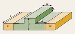
Figure 1. A PN junction was fabricated around the 3-cm-long waveguide. Other dimensions were H = 2.0 μm, h = 0.9 μm, W = 1.5 μm, and d = 1.9 μm.
Now, the researchers who demonstrated the first (pulsed) silicon laser have demonstrated a technique that harvests the energy of the free-carrier current in an external electrical circuit, rather than losing it to heat in the silicon. The investigators from the University of California, Los Angeles, fabricated a 3-cm-long rib waveguide with a PN junction across it (Figure 1). They pumped the waveguide with up to 800 mW at 1539 nm from an amplified diode laser and simultaneously applied an ~4.5-mW signal at the 1673-nm Stokes wavelength. The work was presented at the OSA Topical Meeting on Optical Amplifiers and their Applications, held in Whistler, British Columbia, Canada, in June.
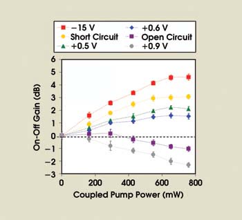
Figure 2. When the junction in Figure 1 was reverse-biased, the free carriers were swept out, so that the absorption loss they caused was reduced to a value lower than the Raman gain; the net gain was positive. But even when the junction was forward-biased with less than 0.7 V, positive net Raman gain was observed.
The researchers observed amplification of the 1673-nm signal when a negative voltage was applied across the junction, sweeping out the free carriers (Figure 2, red squares). This result is similar to what others have observed, but in the current study, the scientists continued to observe optical amplification even when the junction was short-circuited or forward-biased. The power dissipated in the junction was equal to the product of the voltage across the junction and the current passing through it. For the case shown in green triangles and blue diamonds in Figure 2, a positive (forward) voltage produced a negative current. In other words, power was not being dissipated in the junction; instead, the junction was transferring power to the external electrical circuit.
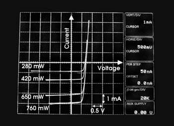
Figure 3. The junction’s electrical characteristics indicate that the current remains negative until the forward bias exceeds ~0.7 V. In this region of negative current and positive voltage, the power dissipated in the junction — the product of current and voltage — is negative. In other words, power is being transferred from the junction to the external electrical circuit.
The electrical characteristics of the junction are shown in Figure 3. For the pumping levels indicated, when the forward voltage was between 0 and ~0.7 V, the junction operated in the lower-right (fourth) quadrant, with a negative current and a positive voltage. It is important to note the physical implication of the negative current: The free carriers are still being swept out of the waveguide, even though it is forward-biased.
Conceptually, the effect can be understood by realizing that power lost from the pump light by two-photon absorption is transferred to the free carriers, and that these carriers create a current that delivers power to the external circuit.
Published: September 2006