Tiny diodes are key to allowing light to interact with light.
Dr. Alistair Poustie, CIP Ltd.
For many years, optics scientists have been looking for all-optical signal processing materials that enable one light beam to be controlled by another. However, most optical materials are linear and allow light beams to pass through without alteration.
The key to achieving all-optical processing functions is to use a nonlinear optical material where different light beams can interact. Of the many nonlinear materials investigated, one device has emerged as a practical solution for all-optical signal processing — the semiconductor optical amplifier (SOA).1
All-optical signal processing is particularly of interest in telecommunications applications, where the benefits of the optical approach in terms of speed, power and cost are becoming important. Today’s telecom networks are based entirely on electronic data handling, but now the core network data speeds are at 40 Gb/s (40 billion bits per second), and, instead of the cheap CMOS silicon devices that formerly handled these signals, specialist electronic materials and sophisticated radio-frequency techniques are required. The electrical signals are also more difficult to route and transmit at these speeds, which require more power and cost more.
In a typical optical transponder today, considerable power is consumed in the detection, processing and retransmission of the optical signals. Modern high-speed electronic switching equipment (such as an IP router rack) can consume more than 10 kW and can require an equivalent power to remove the heat generated by the rack of equipment.
In contrast, all-optical signal processing is intrinsically high speed and can easily handle complex signals and data rates of 40 Gb/s. SOA-based optical processing devices can require much less power (~1 W) than the electronic equivalent (approximately tens of watts) and can be readily integrated to scale to arrays of devices that have smaller footprints. Although the individual tasks that can currently be accomplished with optical processing are relatively straightforward, these tasks — such as wavelength conversion and signal regeneration — are valuable in telecom networks. It is important to understand that all-optical signal processing is not necessarily a replacement for all electronics, but it can greatly increase the effectiveness and capacity scalability of the overall optoelectronic system.
Semiconductor devices
As its name suggests, an SOA is made from semiconductor optoelectronic material (indium phosphide-based) and is pumped electrically to create a population inversion that generates optical gain via stimulated emission (Figure 1). The devices are similar to the familiar semiconductor lasers used in consumer applications (for CD and DVD players) and to the specialist semiconductor lasers that power the optical fiber communications networks worldwide. However, they are designed to be purely amplifiers, not oscillators.
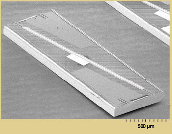
Figure 1. The dimensions of this semiconductor optical amplifier (SOA) are 2000 × 500 × 150 μm. The image was taken with a scanning electron microscope.
One reason that the devices are practical is that they are tiny (volume ~0.1 mm3). A second reason is their high gain (~30 dB), which means that small energies — less than 100 fJ — are required to generate nonlinear effects. For optical communications applications, the device has additional attractive properties, such as being able to couple efficiently to optical fiber and being insensitive to the polarization of incoming signals. The latter is required for operation in real telecom networks because the signal polarization changes as it is transmitted over optical fiber.
The main practical physical mechanisms used for optical nonlinearity in SOAs are cross-gain and cross-phase modulation. There are other useful physical mechanisms, such as four-wave mixing and nonlinear polarization rotation, but these are less favored because of their intrinsic polarization dependence.
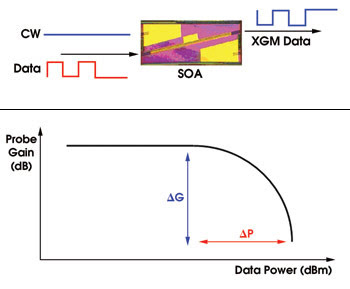
Figure 2. The incoming information carried on one wavelength (represented here in red) is transferred via cross-gain modulation to another wavelength (left). The SOA’s gain at the blue wavelength is saturated by the presence of signalat the red wavelength (bottom) (XGM = cross-gain modulation).
Cross-gain modulation operates as shown in Figure 2. In this simple scheme, the power (ΔP) of the input data signal (red wavelength) causes the gain (ΔG) of the SOA to saturate, and, thus, output power of the second optical input (CW probe beam with blue wavelength) drops. If an optical filter is placed at the output of the amplifier’s output to pass only the blue wavelength, the output signal becomes the logical inverse of the input data. The information on the incoming red wavelength has been converted to the blue wavelength. (Of course, in a telecom system, all wavelengths are in the infrared.) The speed is limited by the gain recovery time of the SOA. This timescale depends on several physical parameters of the device, but recent improvements have shortened the time to less than 25 ps so that wavelength conversion via bit-by-bit cross-gain modulation can be implemented at 40 Gb/s.
Cross-phase modulation is a slightly more complex arrangement than cross-gain modulation, but it is the most widely used because of its potential for higher speed and better performance. In an SOA, whenever the gain is changed, the refractive index of the material changes as well. The change in index is exploited to achieve optical switching by placing the device in an optical interferometer such as the Mach-Zehnder shown on the top of Figure 3. The input data signal (red) changes the gain of the SOA as well as its refractive index.
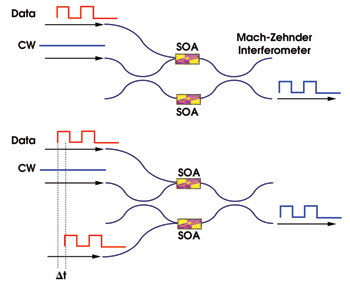
Figure 3. By altering the phase change in one arm of a Mach-Zehnder interferometer, cross-phase modulation can switch the output from one spatial port to the other (top). For higher-speed switching, a delayed signal can be applied to the other arm so that a rapidly saturating gain switches the signal both onto and off the output port of the interferometer (bottom).
If the cross-phase modulation experienced by the blue input beam is π radians, the output light at the blue wavelength is switched from one spatial port to the other. The amplifier can be designed so that the gain change required for a π phase change is only ~5 dB, and the optical power needed for this is less than that required for switching with cross-gain modulation. In addition, the interferometer can provide a much higher extinction ratio on the output data because the amplitude and phase of the light beams interfering at the output can be optimized.
As with cross-gain modulation, the speed of cross-phase modulation effects is limited by the recovery time of the SOA — that is, the time it takes the gain to unsaturate. If higher speeds are required, advanced techniques can be invoked to overcome the device’s gain recovery time. One method, as shown in the lower part of Figure 3, is to time-delay a copy of the input data and to apply that signal to an SOA in the other arm of the Mach-Zehnder. Thus, switching in both directions occurs at the speed of gain saturation. This results in a speed improvement because the gain saturates faster than it unsaturates.
Because of their small physical size, SOAs can be readily fabricated into compact interferometers with a variety of photonic integration approaches. Among these technologies, hybrid integration of the optimized nonlinear SOAs with low-loss silica waveguides (planar lightwave circuits) has been demonstrated to produce high-performance results.2
Practical devices
This integration approach also uses low-cost, passive assembly techniques where the different optical parts are assembled simply by pushing the devices against lithographically defined mechanical stops. This technique has been successful not only for individual SOA-Mach-Zehnder interferometers but also for producing arrays of these devices in a footprint of only a few square centimeters, as part of the EU MUFINS project.3 Figure 4 shows an example of some of the technology used to make these hybrid integrated devices.
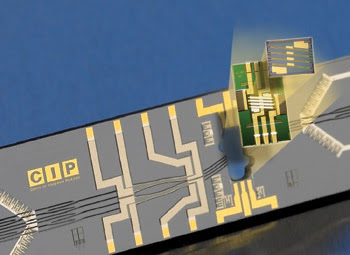
Figure 4. This photomontage shows the hybrid integration assembly of SOAs into a planar lightwave circuit (PLC). The SOA array (top right) solders onto a silicon carrier (middle) that is used to place the SOAs into a machined hole in the PLC (background). The silica waveguides forming the Mach-Zehnder interferometers are the thin black lines running horizontally across the PLC.
Currently there are four main applications for SOA-based all-optical signal processing in telecoms:
• Wavelength conversion.
• Optical regeneration.
• Optical Boolean logic.
• Advanced optical processing circuits.
Wavelength conversion (as shown in Figures 2 and 3) and optical regeneration are useful functions for optical communications systems. Wavelength conversion enables instantaneous wavelength reconfiguration, and regeneration allows transmission over long distances.
Wavelength conversion across the erbium-doped fiber-amplifier wavelength window (nominally 1535 to 1565 nm) has been demonstrated with SOA-based devices at data rates in excess of 40 Gb/s. Figure 5 shows an eye diagram of the high-quality data recorded on a high-speed oscilloscope for wavelength conversion using an SOA-Mach-Zehnder device.4 In this experiment, the required input data optical power was only 1 mW.
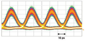
Figure 5. An oscilloscope trace (eye diagram) shows the 40-Gb/s data that has been wavelength-converted from 1549 to 1557 nm using an SOA-Mach-Zehnder interferometer device. The open eye (separation between the logical 1 and 0 levels) indicates that the quality of the output data is high.
Optical regeneration using SOA-Mach-Zehnder devices at 40 Gb/s has shown that almost limitless transmission over optical fiber is possible.5 Most wavelength division multiplexing fiber systems use in-line optical amplifiers (erbium-doped fiber amplifiers) to overcome the optical loss of the fiber and to increase the distance that data can be sent. However, the noise added by the amplifiers also ultimately limits the signal transmission distance. Regeneration with SOA-Mach-Zehnders reduces this noise and allows the optical signals to propagate farther. More research remains to be done to understand how various regenerators using all-optical signal processing can increase the performance and reduce the cost of high-speed optical communications systems.
The ability of all-optical signal processing to scale to more complex processing schemes ultimately depends on using the SOA-based devices to perform combinational optical logic. This application has advanced over recent years, and relatively complex optical circuits using several SOA-based gates have been demonstrated.6 In parallel, the operation speed of the basic SOA-based Boolean gate functions have increased, and up to 85 Gb/s XOR operation has been shown.7
Future benefits
Although it is extremely unlikely that optical signal processing will ever be as complex and powerful as electronic processing, the increased optical functionality would have several benefits for data processing applications. Among these is the ability to directly process optical headers for routing in future optical packet networks and to directly examine high-speed optical header information for optical security algorithm implementation. The latter application is being studied as part of the EU project WISDOM,8 where hybrid integrated optical subsystems based on SOAs are being developed.
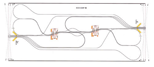
Figure 6. This planar silica waveguide is a time-of-flight optical memory. The chip size is approximately 8 × 4 cm.
One subsystem of interest is an integrated time-of-flight optical memory, such as shown in Figure 6. With this approach, the header bits of interest for packet security are stored by allowing them to propagate around a loop of planar silica waveguide. This data also is regenerated after every round trip to ensure that the signal quality does not degrade. In the security application, the memory capacity storage requirements are modest (a few bytes), but the ability to store and access this 40-Gb/s information with low latency (less than a nanosecond) is key to implementing the security algorithms efficiently.
Meet the author
Alistair Poustie is a research scientist in optical networks and devices at CIP Ltd. in Ipswich, UK; e-mail: [email protected] .
References
1. A. Poustie (March 26, 2007). SOA-based all-optical processing. OFC, tutorial paper OWF1.
2. G. Maxwell (Oct. 30, 2006). Low-cost hybrid photonic integrated circuits using passive alignment techniques, IEEE-LEOS annual meeting, invited paper MJ2.
3. http://mufins.cti.gr
4. G. Maxwell et al (Sept. 29, 2005). WDM enabled, 40Gb/s hybrid integrated all-optical regenerator. ECOC, paper Th4.2.2.
5. O. LeClerc et al (November 2003). Optical regeneration at 40Gb/s and beyond. IEEE J LIGHTWAVE TECHNOL, Vol. 21, pp. 2779-2790.
6. A. Poustie et al (January 2000). All-optical binary counter. OPTICS EXPRESS, Vol. 6, pp. 69-74.
7. X. Yang et al (September 2006). All-optical 85Gb/s XOR using dual ultrafast nonlinear interferometers and Turbo-switch configuration. ECOC, paper Th1.4.2.
8. http://www.ist-wisdom.org.