A beam of individual helium ions creates images that challenge SEM and other microscopy technologies.
Bill Ward, John A. Notte and Nicholas P. Economou, Alis Business Unit of Carl Zeiss SMT
When it comes to imaging at high magnifications, the traditional optical microscope has given way to a number of alternative technologies, each with its advantages and its shortcomings.
One, the scanning electron microscope (SEM), has been around for about 50 years and, compared with its optical ancestors, offers higher-resolution images with longer depths of field. However, advancement in image resolution of the SEM (∼2 nm in practice) has stagnated in recent years, mostly because of electron diffraction and the physics of the interactions between the beam and the sample.
The transmission electron microscope avoids these problems but requires very sophisticated sample preparation. The gallium focused ion beam microscope also offers high resolution, but the large mass of the gallium ions causes considerable sample damage, such as gallium implantation, atomic dislocations and surface sputtering.1 In the special case where it is permissible to contact the sample, there are a number of scanning probe techniques — such as atomic force, scanning tunneling and near-field scanning optical microscopy — that are available for use. Although these images offer excellent resolution, they require some manipulation before the human eye can intuitively interpret them.
A new technology — developed over the past two decades by Bill Ward, now the chief technology officer of Carl Zeiss SMT — avoids some of the pitfalls of each of these methods. The key to the novel system is a helium-ion source that is long-lasting and that provides intense ion currents from a volume no larger than a single atom. The ion source consists of a sharp needle that is maintained under high vacuum in cryogenic temperatures. Applying a high voltage to the needle produces an extremely intense electric field at the needle’s apex. The field is sufficiently strong that any nearby helium atom has an appreciable probability of having an electron tunnel out.
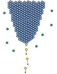
Figure 1. Helium atoms (green) become ionized in the high-field region (orange crescent). The resulting ions (yellow) accelerate away from the tip.
The resulting positive ion then accelerates away from the needle. When the needle is appropriately shaped, the ionization process happens in the vicinity of a single atom at the needle’s apex, and the resulting ion beam appears to emanate from a region less than 1 Å in size (Figure 1). Consequently, the resulting ion beam has a remarkable brightness of 4 × 10⁹ A/cm2/sr. The high brightness is a necessary condition for focusing the beam to a small probe size.2
The helium-ion beam is steered down a column with a series of focusing, alignment and scanning elements that direct it to a probe size as small as 0.75 nm. Much as with an SEM, the beam is rastered across the sample, pixel by pixel. The number of secondary electrons detected determines the gray level of each particular pixel. Because the number of detected secondary electrons varies with material composition and shape, the images provide excellent topographic and compositional information.
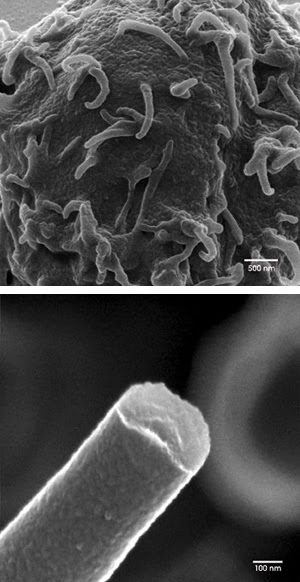
Figure 2. A helium-ion microscope acquired these images of a white blood cell (top)and a carbon nanotube (bottom).
Figure 2 shows two examples of pictures acquired via the helium-ion technology, using an Orion microscope made by Alis Corp., a division of Carl Zeiss SMT — a white blood cell image that depicts topographic and material details and a high-magnification image of a carbon nanotube.
Advantages of helium
Some of the advantages of the helium-ion microscope arise from the properties of the element. Helium atoms are much more massive than electrons, so their de Broglie wavelength is short enough that the focused probe is not affected strongly by diffraction effects. In contrast, most traditional SEMs are limited by the diffraction effects arising from the electron’s wavelike properties.
Helium also is much less massive than gallium (the ion used in most traditional focused ion beams), so there is negligible sputtering or subsurface sample damage. As the helium-ion beam penetrates the sample, there is little scattering; therefore, the images do not suffer from the subsurface blurring effects that are common in SEM images.3 The helium-ion microscope can provide images with higher resolution and more surface-specific information. Figure 3 shows a comparison of an SEM image with a helium-ion microscope image.
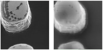
Figure 3. The resolution and contrast of the helium-ion microscope (left) are contrasted with those of a traditional scanning electron microscope (right). The sample is aluminum on silicon.
In addition to images created through secondary electron detection, the incident helium-ion beam offers other opportunities for imaging and analysis. A small fraction of the atoms will be scattered by heavier nuclei and will ricochet out of the sample. The probability of this occurring depends critically upon the atomic number of the scattering nucleus. Therefore, images based on the abundance of scattered helium ions provide a strong elemental contrast that can help distinguish various materials. The image in Figure 4 demonstrates the strong contrast between the chrome and quartz of a photomask. Another advantage of this imaging mode is the strong immunity to charging artifacts resulting from the fact that the scattered helium atoms are not deflected appreciably by these electric fields.
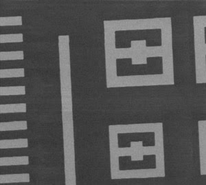
Figure 4. This image of a photomask (chrome on quartz) shows the strong elemental information revealed when detecting scattered helium ions. No charging artifacts are present.
The helium ions also provide crystallographic information. When crystalline domains are viewed, the number of generated ions or electrons depends strongly on the angle of the beam relative to the angle of the crystalline axis. Therefore, differently oriented domains exhibit significantly different contrast. These images make it easy to visualize the sizes and shapes of the grains.
Another imaging mode reveals optical information about the sample. For some materials, photons are produced as the helium-ion beam interacts with the sample. These photons may arise from a cathodoluminescence effect — as also happens with SEMs,4 but another mechanism plays an important role: As a helium ion enters the sample, it captures a free electron and begins the 24.6-eV energy cascade to its ground state. This relaxation process includes the emission of several photons, and their ability to escape from the sample depends crucially on the optical properties of the sample being imaged. Images have been constructed in which the relative abundance of photons is used to establish the gray level. Such images offer nanometer resolution but also reveal optical transparency at the wavelength of interest.
SEMs are equipped with x-ray elemental identification; however, low- and medium-energy helium ions do not produce appreciable x-rays. Fortunately, even without x-rays, helium can be used to provide elemental identification. Helium ions scatter off heavier nuclei, and their scatter angle and energy can determine the mass of the scattering atom. A similar method also provides structural arrangement of the surface atoms. Although this option is unavailable in the commercial helium-ion microscope, the physics is highly developed and well understood. The same analytical principle is used for medium- and low-energy ion scattering and Rutherford backscattering spectroscopy,5 but unlike these techniques, which use ion beams measured in millimeters, the helium-ion microscope provides information at the nanometer scale.
References
1. J. Orloff, M. Utlaut, L.W. Swanson (2002). “Interaction of Ions with Solids.” In: High Resolution Focused Ion Beams, Kluwer Academic/Plenum, pp. 123-146.
2. J. Orloff, ed. (1997). Handbook of Charged Particle Optics, CRC Press, p. 353.
3. L. Reimer (1998). Scanning Electron Microscopy, Springer, pp. 162-165.
4. ibid, pp. 273-288.
5. J.W. Rabalais (2003). Principles and Applications of Ion Scattering Spectrometry, Wiley Interscience.
Meet the authors
Bill Ward is chief technical officer, John A. Notte is director of research and development, and Nicholas P. Economou is chief executive officer of the Alis Business Unit of Carl Zeiss SMT in Peabody, Mass.; e-mail: [email protected].