Lasers enable further miniaturization in electronics by placing tiny components directly into circuit boards.
Scott A. Mathews, Nicholas A. Charipar, Kristin Metkus and Alberto Piqué, US Naval Research Laboratory
Microelectronic circuits traditionally are fabricated by placing packaged components, such as integrated circuits and surface-mount devices, on the surface of a circuit board and connecting the components together. As the demand for miniaturization has grown, however, the size of these packaged components has become a limiting factor.
There are various ways to address this limitation; for instance, application-specific integrated circuits, which eliminate the need for individual components. Instead, the entire circuit is fabricated in one fell swoop and then packaged. However, development of these single-chip designs is costly and time-consuming, and once the chips are completed, their designs are very difficult to change.
A better solution to achieving desired component densities is to place unpackaged components inside the circuit board. These electronic circuits, comprising the embedded components and their interconnects, promise to advance the miniaturization of electronics manufacturing. Embedding components allows a significant reduction of the weight and volume of a circuit. It also leads to shorter interconnects and reduced parasitic inductance, thereby enhancing electrical performance.
Embedding passive components, such as resistors and capacitors, inside a circuit board is not a new technology. However, embedding active semiconductor components has been demonstrated only in specialized applications because the bare semiconductor die are very fragile and tend to be damaged easily by the robotic systems (called “pick-and-place” tools) that mount the devices on a circuit board. Furthermore, pick-and-place tools are ineffective at handling small (less than 1 mm square) or extremely thin (less than 50 μm thick) die, and they are unsuitable also for high-throughput applications (more than 10 devices per second). Avoiding these limitations requires new approaches to the assembly of embedded bare die.
Laser-based device-transfer processes are a novel alternative to conventional mechanically driven pick-and-place methods for placing and embedding millimeter- to micrometer-size structures such as semiconductor bare die, surface-mount and optoelectronic devices, sensors, actuators and microelectromechanical systems (MEMS) onto any surface.
The concept for this process, which we call “lase-and-place,” is simple in principle. Each component is mounted on a laser-transparent support using an intermediate sacrificial polymer layer. Upon exposure to one or several laser pulses, the sacrificial layer is ablated, and the generated vapors release and propel the component away from the support.
Laser-based transfer
Assembly is achieved by aligning the supported device over the pocket where the device is to be embedded. Ultraviolet laser pulses are shaped by an aperture and focused to illuminate an individual device mounted on the support, known as the ribbon. By synchronizing the motion of the ribbon and the receiving substrate underneath with the firing of the laser pulse, it is possible to transfer a given device into a selected pocket, as shown in Figure 1. An imaging system along the path of the laser pulse, represented by the camera in the figure, is used to properly align each device with the pocket in the receiving substrate. This process can be carried out at great speeds (more than 100 devices per second) with accurate lateral precision (within 25 μm) for short travel distances away from the support (about 100 μm).
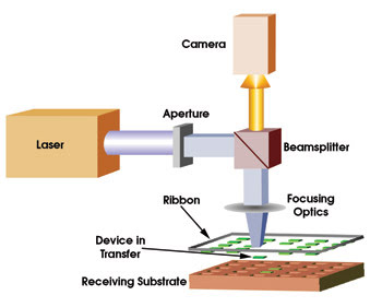
Figure 1. The basic components of a laser pick-and-place system include the laser, the “ribbon” with the components to be placed and the substrate onto which the components will be placed.
The use of laser-based transfer processes for the release and assembly of submillimeter parts initially was studied by Holmes et al.1 The authors demonstrated for the first time the use of laser-transfer processes for the batch assembly of MEMS structures. Despite the success obtained with these, this group did not attempt to apply the process to the transfer of functional semiconductor bare die. At the US Naval Research Laboratory, we recently demonstrated that, by using an ablative UV-laser-transfer process, it is possible to lase-and-place semiconductor bare die without damaging them. The process can transfer devices with sizes ranging from 0.1 up to 10 mm2 onto the surface of a receiving substrate or into previously laser-machined pockets in a plastic or ceramic substrate.2 This process belongs to a class of techniques known as laser direct-write.
Laser direct-write is a general term encompassing several laser-based processes that can create patterns directly on substrates without the use of lithography or masks. These processes can add or subtract materials, modify the materials themselves, and, as already described, transfer complete devices or parts. Laser direct-write processes not only can place the part in a pocket in the circuit board but also can first create the pocket and apply the electrical interconnects to the part after it is in place. Complex patterns in two and three dimensions can be accomplished by translating the ribbon and circuit board and by scanning and modulating the laser beam.
The additive laser direct-write technique has been used with great success to transfer multicomponent liquid or gel systems.3 In these cases, the material to be deposited is suspended or dissolved in a solvent (organic or aqueous), forming a complex fluid, or ink, that is applied as a film onto the transparent ribbon. When the ink absorbs the laser pulse, a small fraction of the volatile solvent vaporizes and propels the remaining ink away from the ribbon.
The transfer of the ink toward the receiving substrate takes place at low laser fluences (<100 mJ/cm2), and, hence, the ink is transferred without significant changes to its properties. Maintaining the ink’s properties is essential when printing electronic inks to form metallic interconnects because it allows patterns deposited on rough or curved surfaces or across steps of varying height to remain continuous and conformal. This laser-printing process has successfully fabricated sensors, microbatteries, interconnects, antennae and solar cells.4
Polymer layer
Using the thin sacrificial polymer layer instead of a volatile solvent to attach individual bare-die semiconductors, surface-mount components or any other part to the transparent ribbon allows release and transfer of the part with a single laser pulse. The key to this process is the selecting and processing of the sacrificial polymer layer. By choosing polymers that fully decompose into volatile by-products when exposed to a laser pulse, it is possible to use the generated vapors to propel a part away from the ribbon. For the transfer to take place in a reproducible fashion and to minimize the possibility of damaging the devices, the sacrificial polymer film must be processed into a thin and uniform layer.
The devices then are placed onto this layer and the polymer cured, thus attaching the devices to the ribbon support. We have used several photopolymers such as photoresists for this purpose. The left side of Figure 2 shows a schematic of the device-transfer process as a function of time, whereas the right side shows stroboscopic micrographs taken at time intervals corresponding to those from the schematic.
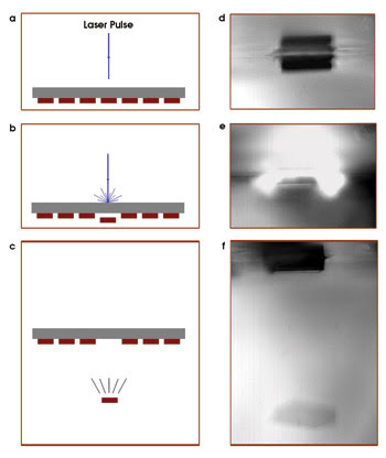
Figure 2. The schematic on the left and the photos on the right show the laser-transfer process as a function of time. The micrographs show the transfer of 1-mm2 silicon substrates. In a and d, the laser pulse has not yet hit the sacrificial polymer layer, and the device is still attached to the ribbon. In b and e, the laser ablates the polymer, causing its vaporization, which results in the ejection of the device from the ribbon. Note the bright flash from the ablated polymer almost engulfing the substrate in e. In c and f, the device is released and travels away from the ribbon toward the receiving substrate (not shown).
The lase-and-place process is a contactless technique and thus allows the transfer of minute and ultrathin devices that easily would be damaged by mechanical pick-and-place tools. In applying this technique to various types of semiconductor bare die, we have demonstrated that it is possible to transfer complete devices with the active surface facing the laser pulse without damage. Hence, the devices are embedded with their contact pads facing up, enabling laser printing of the required interconnects. In Figure 3, the schematic sequence on the left shows the steps involved in laser embedding a device inside a substrate. The photos on the right show a laser-embedded array of LEDs on a flexible polyimide substrate.
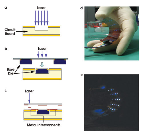
Figure 3. In a to c, the steps required for laser-embedding a device inside a previously laser-machined pocket and then laser-printing the metallic patterns required for interconnecting the device to the rest of the circuit are shown, and in d to e are photographs of a working embedded circuit fabricated using these steps.
The circuit is composed of an array of bare-die blue LEDs each laser-transferred into laser-machined pockets in a 125-μm-thick flexible polyimide substrate. After transfer, a polymer is applied to encapsulate the bare-die LEDs, and lines of silver nano-ink are laser-printed to form the interconnects that are required to address each of the devices individually.
The advantages of the lase-and-place process become apparent when the technique is used to transfer heterogeneous types of devices and components. It is possible to place and assemble dissimilar components or parts onto the same substrate by simply mounting ribbons with different components under the laser beam. This simple capability is not possible with traditional pick-and-place tools, which must be adjusted to accommodate various sizes and shapes. Using the lase-and-place approach, a simple adjustment of the aperture determining the size and shape of the laser beam is all that is required. Totally dissimilar parts ranging from single-LED bare die to micromachined gears can be transferred next to each other with the same tool, merely by changing ribbons (Figure 4). Furthermore, metal patterns can be laser-printed as well, by switching the ribbon to one with a silver ink (Figure 4, right).
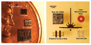
Figure 4. The photo on the left shows bare die of various sizes, placed on a penny for size comparison. The photo on the right shows an arbitrary arrangement of various types of components and parts, all transferred onto a plastic substrate using the lase-and-place process. The artwork in the center corresponds to the laser transfer schematic and was laser-printed using silver metallic nano-ink.
Laser-based transfer techniques such as the one described here allow modification and customization of embedded circuits for specific applications. Moreover, the required circuit layout easily can be reconfigured to fit within a desired form factor. Such capabilities allow the placement of microelectronic systems in places that are beyond the reach of current manufacturing processes. An example of such a need is in the placement of components onto flexible or curved substrates, where there is a need for the fabrication of microelectronic circuits cheaply, cleanly and in precise locations for the next generation of portable, flexible electronics. Much work remains before lase and place reaches the level of sophistication required by the commercial microelectronics manufacturing world; however, its simplicity and versatility make it a promising technique for the assembly of the next generation of microelectronic systems.
Acknowledgments
The authors gratefully acknowledge the support of the Office of Naval Research as well as the contributions of NRL laser direct-write team members Ray Auyeung, Heungsoo Kim and Tom Sutto.
Meet the authors
Scott A. Mathews is a materials engineer at the US Naval Research Laboratory and an assistant professor of electrical engineering at The Catholic University of America; e-mail: [email protected].
Kristin Metkus is a research assistant at the US Naval Research Laboratory; e-mail: [email protected].
Alberto Piqué is a research physicist and head of the electronic and optical materials and devices section at the US Naval Research Laboratory; e-mail: [email protected].
References
1. A. Holmes and S.M. Saidam (1998). Sacrificial layer process with laser-driven release for batch assembly operations. J MICROELECTROMECHANICAL SYSTEMS, Vol. 7, pp. 416-422.
2. A. Piqué et al (2007). Assembly and integration of thin bare die using laser direct-write. SPIE PROC, Vol. 6458, pp. 645802-1–645802-10.
3. C.B. Arnold, P. Serra and A. Piqué (January 2007). Laser direct-write techniques for printing of complex materials. MRS BULLETIN, Vol. 32, pp. 23-31.
4. A. Piqué, H. Kim and C.B. Arnold (2007). Laser forward transfer of electronic and power generating materials. In Laser Ablation and its Applications, C. Phipps, ed.; Springer, pp. 339-373.