A multidisciplinary research effort at Stanford University is focused on developing advanced, lightweight, flexible thin-film solar cells based on abundant and easy-to-process organic materials. This is Part 1 of a two-part series.
Gary C. Bjorklund and Thomas M. Baer, Stanford Photonics Research Center
Global energy consumption is inexorably increasing, driven by population growth and the wave of industrialization in developing countries. Today the world uses about 13 TW of power. Projections are that about 30 TW will be needed by 2050. The sun provides a plentiful, renewable and nonpolluting source of energy. More than 120,000 TW of power from the sun is incident on the Earth. Solar cells produce immediately useful electricity from incident solar radiation and have the potential to be deployed over very large areas to harvest enough power to make a significant contribution to the world’s future energy requirements.
However, there are several important problems that must be solved for solar cells to take on a major role in supplying the world’s electricity. The first is cost. The conventional multicrystalline silicon solar cell modules in use today, at 12 percent efficiency, are just too expensive at $0.27/kWh, in comparison with today’s grid electricity cost of $0.06/kWh.
Besides the module cost, the installation costs are also significant for these crystalline solar modules, in part because of the mechanical structure needed to support their considerable weight. It is important to note that, because of the costs of land, mechanical support structures and ancillary electronics, any new type of solar cell must have at least 10 percent efficiency to be economically viable, even if the cost of the solar cell itself approaches zero.
The second problem is scalability to large areas. Solar cells must be made of low-cost, readily available materials that are present in sufficient abundance to cover hundreds of square kilometers of the Earth’s surface area. They also must be capable of being fabricated on light-weight flexible substrates in large areas by low-cost manufacturing methods — such as roll-to-roll coating — that do not waste materials. Other problems are reliability and lifetime. Alternative solar cell materials must last at least the 20 to 30 years that silicon-based solar cells do today.
Given the ever-increasing demand for energy and the growing concern about the impact of fossil fuel energy sources on the global climate, more and more effort is being directed at developing new solar cell materials and fabrication processes to address these challenges. Solar cell technology development requires combining innovations in nanomaterials, in chemical engineering, and in electrical engineering and photonics — research ideally suited for the university setting, where extensive research programs can be supported in each of these disciplines within multiple departments.
Common meeting ground
At Stanford University, several research groups are exploring paths to meeting these requirements with advanced lightweight, flexible thin-film solar cells based on abundant and easy-to-process organic materials. The principal investigators are faculty members from several departments, including electrical engineering, materials science and engineering, applied physics and chemical engineering. The Stanford Photonics Research Center supplies a common meeting ground for these groups, as well as an interface to commercial companies interested in this dynamic field. Much of the information in this article is drawn from the center’s workshop titled “Solar Cell Technology Options: Paths to Lower $ per Watt” that was held in February.
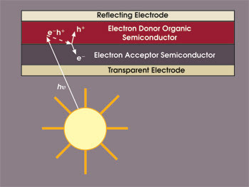
Figure 1. A solar photon creates an exciton, which migrates to the interface between the acceptor and donor. At the interface, the electron and hole separate, creating an electrical current through the solar cell.
Organic thin-film solar cells in their most basic form consist of two layers of semiconducting material sandwiched between a transparent and a reflecting electrode (Figure 1). Sunlight is incident on the cell through the transparent electrode. The electron donor semiconducting material (“the donor”) is always organic and has strong absorption bands that coincide with part of the solar spectrum. It usually is the only layer in the cell that absorbs sunlight. The electron accepting semiconducting material (“the acceptor”) is usually transparent to solar radiation and consists of a material such as carbon-60 or titania (TiO2). The interface between the two semiconductor materials plays a very important role, which is discussed in more detail below. The remaining layers are composed of the transparent electrode, which typically is made from indium tin oxide (ITO), and the reflecting electrode, which is usually a metal such as aluminum.
As opposed to the case of crystalline silicon solar cells, where the free carriers move easily across the layers after they are created by the absorption of photons, in organic semiconductors exciton transport occurs by hopping between individual molecules, a mechanism that is at least four orders of magnitude slower.
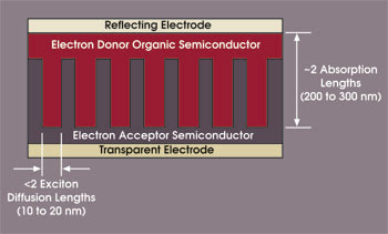
Figure 2. This structure is ideal because any exciton formed in the (red) donor semiconductor is within its diffusion length from the interface. The thickness of the device — several hundred nanometers — is sufficient for good sunlight absorption.
The goal — as well as the challenge — of organic solar cell device design is to separate the electron and the hole before the bound exciton decays. Because the exciton diffusion length is on the order of 4 to 20 nm, the donor and acceptor materials must be structured in such a way that every part of the donor material in the light-absorbing region is within 10 or 20 nm of an interface. Additionally, in an ideal device structure, both the donor material and the acceptor material must have straight pathways back to their respective electrodes to minimize carrier transport time and prevent carrier loss by recombination. Figure 2 shows a schematic of such a structure that provides straight pathways and ensures that the majority of the excitons created are within a diffusion length of an interface.
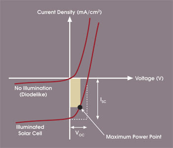
Figure 3. When not illuminated, a solar cell displays the I-V characteristic of any diode. Illumination causes the curve to shift downward so that, when a load resistance is placed across the solar cell, a current flows through it.
The most important means of determining the performance of a solar cell is to measure the current density (I per unit area) that can be produced as a function of the voltage V across the cell, under conditions of illumination equivalent to sunlight. The resulting current density versus voltage curves, known as “I-V characteristics,” typically have the form shown in Figure 3. For zero illumination, the I-V characteristic is the same as the well-known I-V characteristic for a conventional electrical diode: Current flows when it is forward-biased; in contrast, no current (or very little current) flows when it is reverse-biased.
Under conditions of illumination, the I-V characteristic shifts downward by an amount ISC so that I = –ISC when V = 0. ISC is known as the “short-circuit current” because V = 0 is equivalent to a short circuit. This downward shift in the I-V characteristic causes V to have a nonzero value VOC when I = 0. VOC is known as the “open-circuit voltage” because I = 0 is equivalent to an open circuit. The solar cell generates power for all values of I and V that correspond to the portion of the I-V characteristic that is in the lower right-hand quadrant of the graph (V > 0, I > 0). In principle, the data in the lower right quadrant could be obtained simply by placing a variable load resistance across the diode, whereas obtaining the data in the other quadrants would require an external voltage to be supplied.
The most important parameters to be extracted from the I-V characteristic are the short-circuit current (ISC), the open-circuit current (VOC) and the so-called “fill factor.” A larger product, ISC * VOC, implies higher output power from the device. The maximum power that can be produced by the solar cell is given by the point on the curve where the product I * V is a maximum. The fill factor is the ratio of this product to the product ISC * VOC. Graphically, the fill factor is the ratio of the area of the colored rectangle to the area of rectangle defined by the dotted lines. The efficiency of a solar cell is the power produced by the cell at the maximum power point divided by the power of the incident radiation under standard test conditions.
Polymer organic solar cells
Professor Michael D. McGehee, a faculty member in the department of materials science and engineering at Stanford University, studies the underlying physics of solar cell materials and nanostructured materials, as well as the critical and practical requirements of the material properties necessary for cost-effective manufacturing. He is well-suited for this approach, with degrees in both physics and materials science. He has done pioneering work on nanostructured solar cells using semiconducting polymers as the light-absorbing electron donors.1,2
These materials have direct bandgaps, and, hence, interact with light so strongly that films only 100 to 500 nm thick are needed for efficient absorption, in contrast to the 100-μm thicknesses needed in crystalline silicon. This allows the use of very thin films requiring small amounts of the active material.
These semiconducting polymers share many of the mechanical durability and processing advantages of polymers in general. They can be dissolved in a variety of solvents and placed onto flexible substrates under ambient temperature and pressure using well-known wet-processing techniques such as spin casting, dip coating, ink-jet and screen printing, and micromolding. Scalability to large areas with little materials loss is possible, and roll-to-roll coating techniques can be used. Roll-to-roll coating, where the flexible substrate to be coated is played out from one roll, passed through a coating chamber and, after being coated, spooled onto another roll, has been shown to be a highly cost-effective continuous manufacturing process in industries such as paper, food packaging and photographic film.
Porous titania
A promising approach to the realization of the ideal device structure that was shown in Figure 2 involves the use of porous titania (TiO2) as the electron-acceptor material. TiO2 can be patterned into a continuous network for electron transport that contains numerous pores into which the semiconducting polymer material can be infused to form a coexisting continuous network for hole transport. Although this structure does not always provide a direct path for the electrons and holes to their respective electrodes, it is still better than the planar interface of Figure 1.
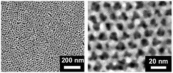
Figure 4. Uniform 8-nm pores in this TiO2 film provide a structure that is a step toward the ideal described in Figure 2.
Figure 4 shows a TiO2/polymer structure created in McGehee’s group using mesostructured TiO2 formed using block copolymer synthesis techniques. The resulting TiO2 layer has numerous highly uniform 8-nm pores that penetrate to the bottom of the layer. As shown in Figure 5, a semiconducting polymer was melt-infiltrated into the pores of the TiO2 by spinning a film of the polymer on top of the TiO2 layer and heating the sample. The short-circuit current (ISC) obtained from solar cells made with mesoporous TiO2 was more than three times greater than that generated from cells with flat TiO2.
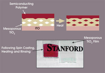
Figure 5. The semiconducting polymer is spun on top of the porous layer of titania, and the sample is heated. The molten polymer is drawn into the pores in the titania.
Recently, McGehee and his group explored the use of carbon-nanotube networks as flexible transparent electrodes for thin-film organic solar cells.3,4 Today’s transparent electrodes use materials such as ITO that have limited availability, are relatively brittle, require vacuum and heat processing, suffer from delamination and chemical compatibility issues, and are relatively costly. The ideal transparent electrode material would have high sheet conductivity and greater than 90 percent transparency, be made of abundant and nontoxic materials, be flexible and have good adhesion, and be cheaply processible in a way that is compatible with organic materials. Carbon-nanotube networks have the potential to be significantly superior in performance as well as less expensive than ITO.
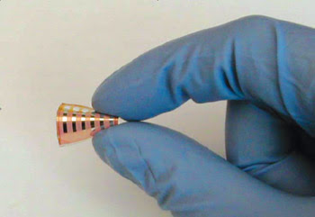
Figure 6. This flexible thin-film solar cell has a semiconducting polymer active layer and a carbon-nanotube-network transparent electrode.
Preliminary experimental results with the carbon-nanotube networks are encouraging. In the area of flexibility and adhesion, carbon-nanotube-network electrodes clearly outperformed ITO. Solar cells on flexible polymer substrates could be bent to 5-mm curvature with no degradation using carbon-nanotube electrodes, while similar solar cells using ITO electrodes were destroyed at this bending radius. Efficiency results also are promising, with the first carbon-nanotube solar cells achieving 2.5 percent efficiency, as opposed to 3.0 percent for ITO solar cells. Figure 6 shows an example of a flexible carbon-nanotube solar cell fabricated by McGehee’s group.
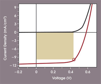
Figure 7. The top curve shows the I-V characteristic of a solar cell made from a blend of semiconducting polymers, as measured in the dark. The bottom curve shows the I-V characteristics when the cell is illuminated with standard solar irradiance. The open circle shows the maximum power point, and the shaded rectangle represents the fill factor.
The most efficient polymer organic solar cells that have been produced by his group use a blend of semiconducting polymers with different bandgaps. Figure 7 shows I-V characteristics for one such cell. This cell achieved an efficiency of 4.33 percent at the maximum power point with a fill factor of 65 percent. The group is using x-ray diffraction, spectroscopy, conducting atomic force microscopy and transport measurements coupled with numerical device simulations to better understand what limits the efficiency of this device.
This concludes Part 1 of this two-part article. Part 2 will provide a description of the research being conducted at Stanford by professor Peter Peumans’ group on small-molecule organic solar cells and by professor Zhenan Bao’s group on new organic materials for solar cells. It will conclude with a discussion of the prospects for developing organic solar cells with power conversion efficiency that is competitive with that of amorphous silicon solar cells.
Acknowledgment
Michael D. McGehee’s work is sponsored by the Global Climate and Energy Project, by the US Department of Energy and by the National Science Foundation Center for Polymer Interfaces and Macromolecular Assemblies.
Meet the authors
Gary C. Bjorklund is consulting director for Solar Cells, Telecom and Information Technology at Stanford Photonics Research Center; e-mail: [email protected].
Thomas M. Baer is the executive director of Stanford Photonics Research Center; e-mail: [email protected].
References
1. M.D. McGehee et al (Feb. 24, 2007). Improving organic solar cells. SPRC Workshop: Solar Cell Technology Options: Paths to Lower $ per Watt, Stanford University, Stanford, Calif.
2. K.M. Coakley and M.D. McGehee (Nov. 16, 2004). Conjugated polymer photovoltaic cells. CHEM MATER, pp. 4533-4542.
3. M. Topinka et al (Feb. 24, 2007). Carbon nanotube electrodes for solar cells. SPRC Workshop: Solar Cell Technology Options: Paths to Lower $ per Watt, Stanford University, Stanford, Calif.
4. M.W. Rowell et al (June 5, 2006). Organic solar cells with carbon nanotube network electrodes. APPL PHYS LETT, 233506.