
Silicon Lasers Approach Mid-IR
Silicon-chip-based lasers developed at Intel Corp. that exploit "cascaded Raman lasing" could extend the wavelength of silicon laser operation from the near- to the mid-infrared (IR).
Cheap and powerful semiconductor lasers that operate in that region (2 to 5 µm) are highly sought for applications such as medical diagnostics and environmental monitoring. The Intel team's research may make them possible.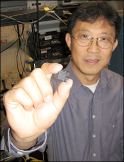
Haisheng Rong, PhD, a senior research scientist in the Photonics Technology Lab of Intel's Corporate Technology Group, lead the team that demonstrated the longest wavelength reported for silicon Raman lasers. (Photo: Intel)
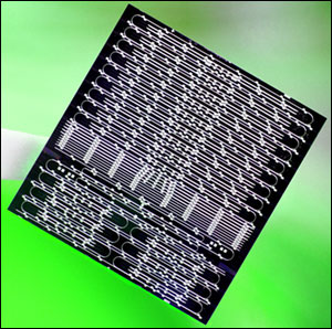
Although silicon Raman lasers have been made before, their wavelength of operation has always been limited to around 1.6 µm. Haisheng Rong and colleagues have demonstrated it is possible to create a silicon-chip laser that emits mW-scale powers at a wavelength of 1.848 µm.
This is the longest wavelength reported so far for silicon Raman lasers, and it is "tantalizingly close to the mid-infrared window," the researchers said -- offering hope that by optimizing the design, it should be possible to make lasers that operate at even longer wavelengths and open up even more, as yet undiscovered, applications, including defense and biological uses such as lab-on-a-chip technology.
The new technology platform offers promising low-cost optoelectronic solutions for applications such as telecommunications, chip-to-chip interconnects, optical sensing and biomedical applications.
"More and more photonic devices and functions have been developed on silicon platforms, and the scope of their applications is ever expanding," Rong said in an Intel blog post.
The cascaded silicon Raman laser’s new sensing capabilities were demonstrated by measuring greenhouse gasses, methane gas and water vapor, to identify their molecular fingerprints.
The demonstration establishes a pathway to extending the laser wavelength into the mid-IR region for gas sensing and other important spectroscopy applications that are now possibly only with bulky, expensive or cryogenically cooled lasers, said Mario Paniccia, PhD, a member of the research team and director of the Silicon Photonics Technology Lab at Intel.
Paniccia, who has been director of the lab since 2000, said the idea for the demonstration arose from a simple question: "I couldn't understand why these things were so expensive," he said. "I thought it would cost a lot less in silicon."
Most lasers are based on light amplification by stimulated emission of radiation predicted by Einstein, but a special category of laser is based on stimulated Raman scattering. A major attraction of Raman lasers is their ability to use light from an optical “pump” to generate coherent light emission in wavelength regions that are hard to reach with conventional types of lasers. In addition, Raman lasers can be made from materials such as silicon that do not possess suitable energy band structures to produce laser light by stimulated emission.
"Cascaded lasing is a unique attribute of Raman lasers," Rong said. "A Raman laser’s output beam -- which is always at a longer wavelength than the pump -- can itself act as a pump to generate Raman lasing at an even longer wavelength. This so-called cascaded process can continue to generate longer wavelengths."
A cascaded Raman laser can be realized by properly designing the laser cavity to take advantage of this unique property, he said. "Cascaded lasing enables a Raman laser to have greater wavelength coverage, and one can use a low-cost and efficient laser as a pump to generate coherent light in longer wavelength region where it is difficult to achieve lasing by other methods."
Three years ago, researchers from Intel’s photonics technology lab demonstrated the first continuous-wave (CW) silicon Raman laser.
Since then, Rong said, they have made major improvements. "Instead of applying optical coatings on the chip facets to form a laser cavity, we designed a 'mirror-less' ring cavity laser which is monolithically integrated on a chip and fabricated entirely in a CMOS fab. We have achieved 10 times reduction in lasing threshold to below 20 mW and 5 times increase in output power to more than 50 mW."
This cavity design is scalable to enable size reduction and can be integrated with other silicon photonic components on the same chip, he said.
"Another significant characteristic of the silicon Raman laser is its extraordinary spectral purity," he added. This is very important for many laser applications such as high-resolution spectroscopy."
Rong said these improvements led to the current breakthrough in achieving cascaded Raman lasing in silicon.
"These results demonstrate that the performance of the cascaded silicon Raman laser in terms of power, stability and wavelength tunability is suitable for practical applications even in its current development phase," Rong said. "In addition to its low-cost material and CMOS compatible fabrication aspects, the cascaded silicon Raman laser offers unique advantages such as wavelength selectivity and spectral purity that can compete with complex and bulky solid state laser systems, but in the small form factor of semiconductor lasers. Single-mode, room-temperature operation is obtained from a monolithic chip without the extra cost associated with additional cavity components and their assembly and alignment."
He said the spectral coverage of silicon Raman lasers could be further extended by higher orders of cascaded lasing.
"A theoretical study has shown that up to 6th order cascaded lasing may be possible," Rong said. "The unique features of this new type of laser, combined with its low-cost fabrication and optoelectronics integration potential, could enable an entire new suite of devices and applications in the near and mid IR spectral region."
Paniccia said the team's new research "opens up what Moore's Law [regarding the dramatic increase in the usefulness of digital electronics] has done. And once the systems reach certain price points, new uses will be discovered that no one can predict. It's a testament to the rate of advancement in this field that silicon can now be considered an optical material."
Right now, Paniccia said, the demonstration is in the realm of a scientific breatkthrough. "We've proven we can build it; we'll now be looking at commercialization."
The research is described in paper, “Cascaded silicon Raman laser” (Haisheng Rong, Shengbo Xu, Oded Cohen, Omri Raday, Mindy Lee, Vanessa Sih and Mario Paniccia) published online by Nature Photonics.
For more information, visit www.intel.com/go/sp/
/Buyers_Guide/Intel_Corp/c6919