By combining techniques, manufacturers can conduct fast, nondestructive measurement and analysis functions.
Matt Smith, Olympus Surgical Industrial America Inc.
The field of industrial microscopy has evolved from simple bright-field on-axis imaging to that of nonvisible and confocal-based technologies. Bright-field is a resolution-limited technique that uses on-axis illumination and imaging to form the image, typically with visible light. Confocal microscopy allows improved contrast and resolution as well as an extremely small depth of focus. By combining confocal with nonvisible techniques, researchers now can look through certain materials to see inside devices such as microelectrical mechanical systems (MEMS).
In fact, the MEMS industry has been the driving force behind this evolution. The semiconductor manufacturing industry requires improved efficiency and resolution, both of which are addressed with near-IR (800-1500 nm), deep-UV (248 nm) and confocal imaging technologies.
Looking inside with near-IR
Near-IR imaging has become essential to semiconductor manufacturers that use silicon as the substrate because silicon has an excellent transmission capability for the near-IR spectrum. By using an optical system optimized for this wavelength band in conjunction with calibrated image analysis software, images and measurements can be made in seconds. For further flexibility, an IR capability can be retrofitted to many existing microscope systems and can be used without removing any key components from a standard optical system. The optical design of the microscope must be fine-tuned and the optics coated to optimize the contrast and transmission of the nonvisible wavelengths (Figure 1).

Figure 1. Silicon and other substrates have excellent transmission at near-IR wavelengths, making near-IR microscopy the technique of choice for many sensor manufacturers for inspecting and aligning wafers.
Near-IR is used in MEMS manufacturing and in wafer bonding to view the interior of a device to make sure it is sound and fault-free. This is possible because of the transparency of silicon and other substrates at near-IR wavelengths. Using near-IR, fast nondestructive inspection and measurement can be carried out in minutes without the need for any time-consuming or costly sample preparation.
Additional demands from the MEMS market are for improved resolution and surface imaging as a result of geometries that are decreasing in overall size. Thus, deep-UV imaging, which allows examination of many fine details measuring down to less than 0.10 μm, has become increasingly popular for this application. As with the near-IR technique, deep-UV requires no sample preparation and is fast, particularly when compared with scanning electron microscopy, where queue time can delay important results.
Much like the IR system, a deep-UV optical system can be added in a modular manner and can be retrofitted and used in conjunction with bright-field and other conventional imaging techniques without any disruption of normal microscope operation (Figure 2).
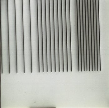
Figure 2. Deep-UV illumination shows details down to less than 0.10 μm.
Another emerging technique is confocal microscopy. It provides improved horizontal measurements and, with its small depth of field, enables Z-axis measurements. Z-axis measurements smaller than the depth of focus are possible by using intensity-profile interpolation along with ultrafine positioning techniques. Fast and simple Z-axis measurements of characteristics such as roughness can be performed without sample preparation. When compared with a stylus system, the confocal technique provides almost instant results with higher precision. It also is noncontact, so that fragile or sensitive samples can be measured without damaging the part.
Z-axis measurements
One method of confocal microscopy uses a scanning laser diode to illuminate the sample. For example, a laser confocal microscope using a 408-nm laser provides improved resolution of 120 nm horizontally. This microscopy method can be combined with intensity profiling, which examines the signal strength in relation to location to interpolate the peak position — information in turn used to determine the exact point of optimum focus. When intensity profiling is combined with the confocal technique, displacements as little as 20 nm in the Z-axis can be achieved. Laser scanning confocal microscopy can generate Z-axis data that provides topographic and roughness information directly comparable to that measured using interferometers and stylus-based roughness testers. Unlike scanning electron microscopy, the sample requires no preparation. The data can be generated in minutes and requires no advanced interpretation by the operator, as is often needed with interferometers (Figure 3).
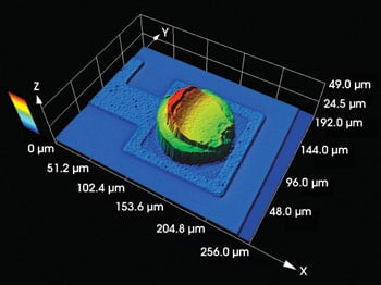
Figure 3. Confocal technology can generate topographic and roughness details, as shown here with X-, Y- and Z-dimensional data.
Further aiding the growing number of MEMS manufacturers is the fact that the confocal technique also can be performed in the near-IR region. The basic technology remains the same as for visible-light confocal; however, a 1310-nm wavelength is used. Because of the transparency of silicon, repeatable and accurate measurements can be made through the silicon base at this wavelength to measure whether the wafer has bonded. This technique likewise requires neither sample preparation nor advanced interpretations by the operator, both of which are sometimes required for ultrasonic tools designed for opaque substrate measurement.
The emergence of these new and varied imaging techniques has created the need for a tool to organize and archive the important data generated by various instruments. Advanced database systems receive images and data from near-IR and deep-UV digital camera inputs and receive information generated by the laser confocal tools. Additionally, it’s beneficial for database systems to adapt to scanning electron microscopes, to atomic force microscopes, or to any other image-generating system so that the data is integrated into a single database for sharing within one facility or with other facilities around the world.
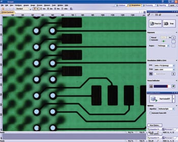
Figure 4. By using a dedicated application, images and data can be gathered and centrally stored.
Although the demand for conventional white-light microscopy continues to remain robust in industry, the new and evolving needs of high-technology manufacturers of MEMS and other microstructure technologies have required innovation outside the visible area. Near-IR and deep-UV offer safe and nondestructive solutions that provide both images and data. The new laser confocal systems provide a faster, less demanding method of generating topographic data without the need for sample preparation or interpretation. Regardless of the technique, all of the data now can be centrally stored and retrieved with the use of advanced image database tools to provide fast and cost-efficient imaging and data retrieval across a single facility or among multiple facilities (Figure 4).
Meet the author
Matt Smith is director of sales and marketing at Olympus Surgical, Industrial America, Micro Imaging Div., in Orangeburg, N.Y.; e-mail: [email protected].